

electronics-journal.com
06
'26
Written on
Modified on
Fraunhofer News
OLED Microdisplay Interface Integration for Wearable Near-Eye Display Systems
Fraunhofer IPMS engineers a 2K OLED microdisplay package integrating MIPI DSI-2 control and onboard power management.
www.fraunhofer.de
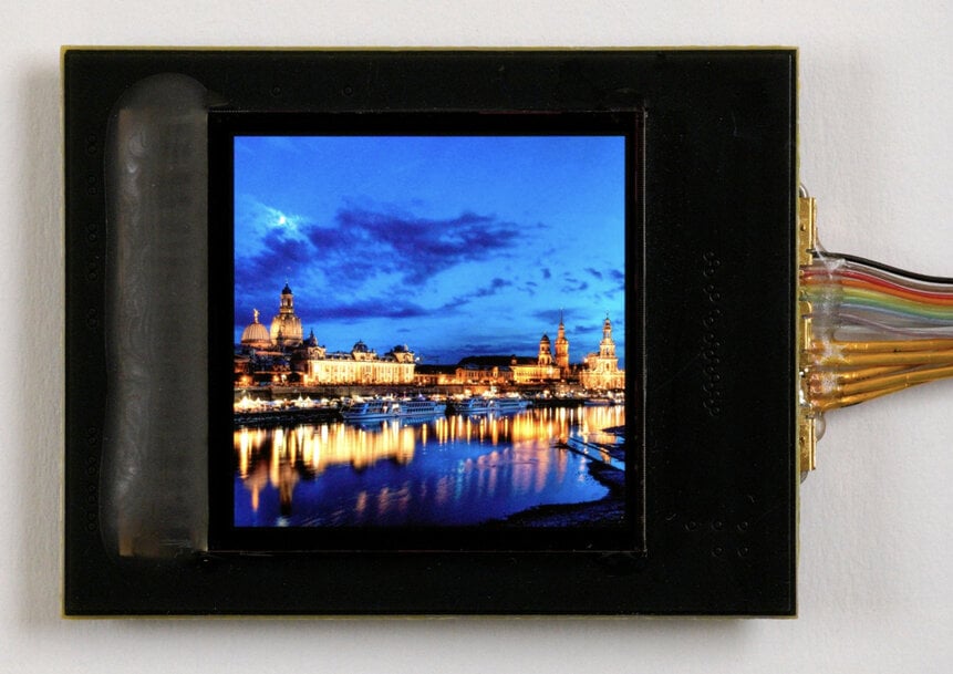
© Fraunhofer IPMS: 2K OLED microdisplay package with integrated MIPI DSI-2 control (2048 x 2048 pixels, 1.07 inches).
Optical system designers and wearable hardware engineers face PCB layout constraints and routing complexity when driving high-resolution microdisplays within compact smart glasses, head-mounted displays, and industrial helmets. The Fraunhofer Institute for Photonic Microsystems IPMS addresses these physical and electrical bottlenecks with a compact packaging architecture for its 2K OLED microdisplay, embedding native MIPI DSI-2 serial connectivity alongside internal power generation circuitry.
Embedded System-on-Module for High-Bandwidth Display Control
Integrating high-resolution organic light-emitting diode (OLED) microdisplays into head-mounted optical systems typically requires supplementary multi-voltage power supplies and external bridge chips to convert digital video from application processors into panel-compatible formats. These multi-chip configurations expand the Bill of Materials (BOM), increase thermal dissipation in proximity to the user's temple, and complicate flexible printed circuit (FPC) routing across spatial limits.
The Fraunhofer IPMS packaging design resolves these integration hurdles through an integrated 20 mm x 20 mm system-on-module (SoM). The module incorporates a MIPI DSI-2 interface operating via a D-PHY physical layer, an established protocol in mobile application processors that transmits packetized video streams and panel initialization commands across high-speed differential pairs. Supporting up to four physical data lanes running at up to 2.5 Gbit/s per lane, the interface provides up to 10 Gbit/s of total bandwidth, eliminating off-board bridge silicon.
Onboard Voltage Generation and Signal Harmonization
Beyond protocol serialization, OLED microdisplays require multiple dedicated supply rails to power underlying CMOS active-matrix backplanes, gate drivers, column drivers, and common cathode configurations. The integrated SoM contains onboard power management components that synthesize all required internal bias and driving voltages from a single external 5 V power rail.
In wearables like smart glasses and display helmets, interior layout volume is restricted, explains Florian Schuster, project manager at Fraunhofer IPMS. The packaging was engineered to house the drive electronics within the baseline package dimensions, combining the small form factor with simplified electrical integration. By drawing power from a single 5 V line, the integrated MIPI DSI-2 controller removes external interface conversion requirements. This architecture expands the institute's previous microdisplay interfacing options, which relied on Low-Voltage Differential Signaling (LVDS) and Display Pixel Interfaces (DPI).
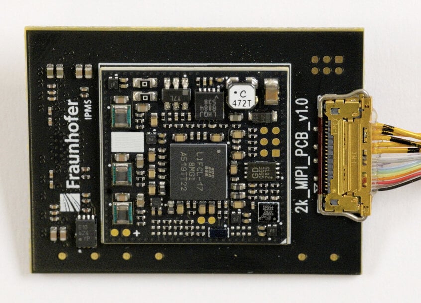
© Fraunhofer IPMS: 2K OLED microdisplay package with integrated MIPI DSI-2 control (20 x 20 mm SoM).
High-Density Substrate Integration and Evaluation Kits
Accommodating active silicon, passive decoupling components, power regulation arrays, and differential routing without enlarging external packaging dimensions required high-density interconnect (HDI) circuit design. Fraunhofer IPMS plans to extend this embedded package architecture to other microdisplay resolutions across its technology portfolio.
The hardware implementation was validated in bench testing using a Raspberry Pi 5 platform. To accelerate prototype development and optical benchmarking, Fraunhofer IPMS supplies evaluation kits containing the fully packaged 2K OLED microdisplay, an integrated driver board with preconfigured software drivers, and interface cabling. The microdisplay package will be presented at SEMICON Europa 2026, held November 10–13, 2026, in Munich, Germany, at the Silicon Saxony joint pavilion in Hall B1, Booth B1-221-25.
Additional Context:
This section details technical specifications and competitive benchmarking not included in the original product announcement.
The underlying Fraunhofer IPMS 2K microdisplay features a 1.07-inch diagonal active matrix with a square format of 2048 x 2048 pixels and a 9.3 µm x 9.3 µm RGB-stripe pixel pitch, fabricated on a high-voltage silicon CMOS backplane. In the competitive landscape for near-eye OLED-on-Silicon (OLEDoS) hardware, commercial panels from manufacturers such as Sony Semiconductor Solutions (e.g., the ECX339A 0.5-inch UXGA) typically utilize proprietary sub-LVDS or MIPI D-PHY interfaces requiring external companion PMICs to generate multiple asymmetric analog voltages (such as +10 V, -4 V, and +1.8 V logic rails). Standard MIPI DSI-2 v1.1 running over D-PHY v1.2/v2.0 achieves maximum operational efficiencies around 2.5 Gbit/s per lane, yielding sufficient throughput to drive 2048 x 2048 arrays at 60 Hz to 90 Hz with 24-bit RGB depth without visual compression artifacts, providing a streamlined drop-in pathway for Qualcomm Snapdragon XR and modern ARM-based embedded host processors.
Edited by Natania Lyngdoh, Induportals editor, with AI assistance.
www.ipms.fraunhofer.com
Optical system designers and wearable hardware engineers face PCB layout constraints and routing complexity when driving high-resolution microdisplays within compact smart glasses, head-mounted displays, and industrial helmets. The Fraunhofer Institute for Photonic Microsystems IPMS addresses these physical and electrical bottlenecks with a compact packaging architecture for its 2K OLED microdisplay, embedding native MIPI DSI-2 serial connectivity alongside internal power generation circuitry.
Embedded System-on-Module for High-Bandwidth Display Control
Integrating high-resolution organic light-emitting diode (OLED) microdisplays into head-mounted optical systems typically requires supplementary multi-voltage power supplies and external bridge chips to convert digital video from application processors into panel-compatible formats. These multi-chip configurations expand the Bill of Materials (BOM), increase thermal dissipation in proximity to the user's temple, and complicate flexible printed circuit (FPC) routing across spatial limits.
The Fraunhofer IPMS packaging design resolves these integration hurdles through an integrated 20 mm x 20 mm system-on-module (SoM). The module incorporates a MIPI DSI-2 interface operating via a D-PHY physical layer, an established protocol in mobile application processors that transmits packetized video streams and panel initialization commands across high-speed differential pairs. Supporting up to four physical data lanes running at up to 2.5 Gbit/s per lane, the interface provides up to 10 Gbit/s of total bandwidth, eliminating off-board bridge silicon.
Onboard Voltage Generation and Signal Harmonization
Beyond protocol serialization, OLED microdisplays require multiple dedicated supply rails to power underlying CMOS active-matrix backplanes, gate drivers, column drivers, and common cathode configurations. The integrated SoM contains onboard power management components that synthesize all required internal bias and driving voltages from a single external 5 V power rail.
In wearables like smart glasses and display helmets, interior layout volume is restricted, explains Florian Schuster, project manager at Fraunhofer IPMS. The packaging was engineered to house the drive electronics within the baseline package dimensions, combining the small form factor with simplified electrical integration. By drawing power from a single 5 V line, the integrated MIPI DSI-2 controller removes external interface conversion requirements. This architecture expands the institute's previous microdisplay interfacing options, which relied on Low-Voltage Differential Signaling (LVDS) and Display Pixel Interfaces (DPI).
© Fraunhofer IPMS: 2K OLED microdisplay package with integrated MIPI DSI-2 control (20 x 20 mm SoM).
High-Density Substrate Integration and Evaluation Kits
Accommodating active silicon, passive decoupling components, power regulation arrays, and differential routing without enlarging external packaging dimensions required high-density interconnect (HDI) circuit design. Fraunhofer IPMS plans to extend this embedded package architecture to other microdisplay resolutions across its technology portfolio.
The hardware implementation was validated in bench testing using a Raspberry Pi 5 platform. To accelerate prototype development and optical benchmarking, Fraunhofer IPMS supplies evaluation kits containing the fully packaged 2K OLED microdisplay, an integrated driver board with preconfigured software drivers, and interface cabling. The microdisplay package will be presented at SEMICON Europa 2026, held November 10–13, 2026, in Munich, Germany, at the Silicon Saxony joint pavilion in Hall B1, Booth B1-221-25.
Additional Context:
This section details technical specifications and competitive benchmarking not included in the original product announcement.
The underlying Fraunhofer IPMS 2K microdisplay features a 1.07-inch diagonal active matrix with a square format of 2048 x 2048 pixels and a 9.3 µm x 9.3 µm RGB-stripe pixel pitch, fabricated on a high-voltage silicon CMOS backplane. In the competitive landscape for near-eye OLED-on-Silicon (OLEDoS) hardware, commercial panels from manufacturers such as Sony Semiconductor Solutions (e.g., the ECX339A 0.5-inch UXGA) typically utilize proprietary sub-LVDS or MIPI D-PHY interfaces requiring external companion PMICs to generate multiple asymmetric analog voltages (such as +10 V, -4 V, and +1.8 V logic rails). Standard MIPI DSI-2 v1.1 running over D-PHY v1.2/v2.0 achieves maximum operational efficiencies around 2.5 Gbit/s per lane, yielding sufficient throughput to drive 2048 x 2048 arrays at 60 Hz to 90 Hz with 24-bit RGB depth without visual compression artifacts, providing a streamlined drop-in pathway for Qualcomm Snapdragon XR and modern ARM-based embedded host processors.
Edited by Natania Lyngdoh, Induportals editor, with AI assistance.
www.ipms.fraunhofer.com
