
electronics-journal.com
25
'22
Written on Modified on
PCB Pattern Design for ESD Countermeasures and ESD Visualization
TDK has a lineup of multilayer chip varistors that protect equipment for malfunction and failure due to ESD (electrostatic discharge), and we have long contributed to solving customer ESD problems.
Recently, however, although multilayer chip varistors have been effective in the past, they have been unable to provide sufficient protection as customer devices have become smaller, lighter, and more sophisticated. To investigate the cause of this problem, we conducted ESD tests assuming the miniaturization of customer equipment.
Background
The shift to 5G will enable interoperability in real-time communication between devices, and all types of devices are required to have higher quality design, such as smaller size and lighter weight, lower power consumption, higher functionality, longer operating time, higher reliability, and improved EMC tolerance.
The board and body designs of devices differ between large devices such as automobiles, industrial equipment, and medical devices, and small mobile devices such as smartphones, VR equipment, and drones. Small mobile devices are among the most difficult to protect against ESD because the board size cannot be increased, ESD can easily penetrate, in the GND patterns and body used to release ESD are often unstable.
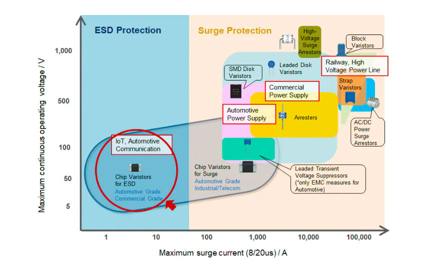
TDK has an extensive lineup of varistors (zinc oxide) and arrestors (discharge tubes) for use as voltage protection elements. These components can be used for various applications ranging from low to high current. The ESD test described in this article uses the chip varistors shown in the product map below for ESD protection Click on the product for details
Test Objective
Use a PCB with a different GND pattern design and use the ESD visualization system to confirm how ESD is bypassed to the GND pattern through ESD protection components when ESD is applied.
Assumed Conditions
1. Due to the miniaturization of equipment, the PCB size cannot be more larger.
2. The GND pattern cannot be wider.
3. The GND pattern of the PCB is not connected to the metal shield.
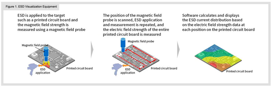
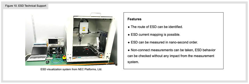
ESD Visualization Equipment
The ESD visualization equipment is a device that can make electrostatic discharge (ESD) current visible by automatically scanning using a non-connect magnetic field probe.
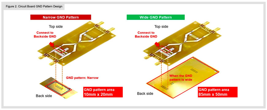
Circuit Board GND Pattern Design
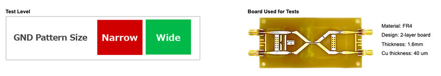
For the tests, a two-layer board (Top : signal pattern; Back: GND pattern; the GND pattern on the top is connected to the back by via).
Each GND pattern on the back side has a different area, and two types are available: (1) a narrow pattern (10 x 20 mm), and (2) a wide pattern (85 x 50 mm).
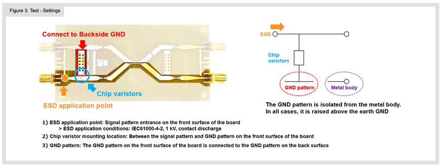
Test - Settings
A chip varistor was placed on the top layer between the signal pattern and the GND pattern. The GND patterns are isolated from the metal body and the earth GND. In this state, ESD 1kV was applied to the signal pattern under IEC 61000-4-2 conditions.
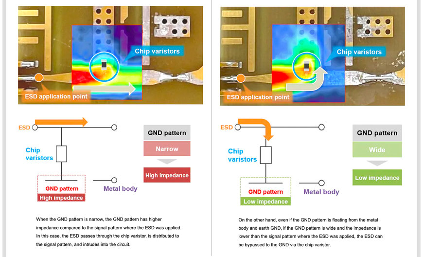
Test - Measurement Results
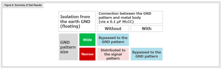
When the GND pattern is narrow, the ESD passes through the varistor and is distributed to the signal pattern. On the other hand, when the GND pattern is wide, the ESD passes through the varistor and is bypassed to the GND pattern.
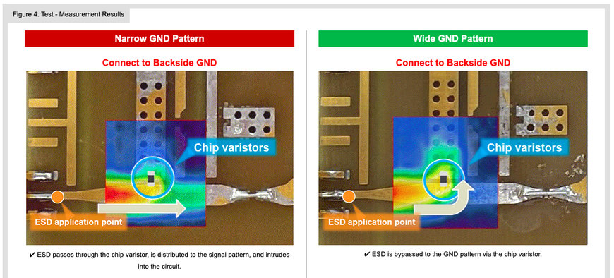
This depends on the magnitude of impedance of the GND pattern with respect to the signal line. If the GND pattern is narrow, the impedance on the GND side becomes higher, and the ESD cannot be bypassed via the chip varistor.
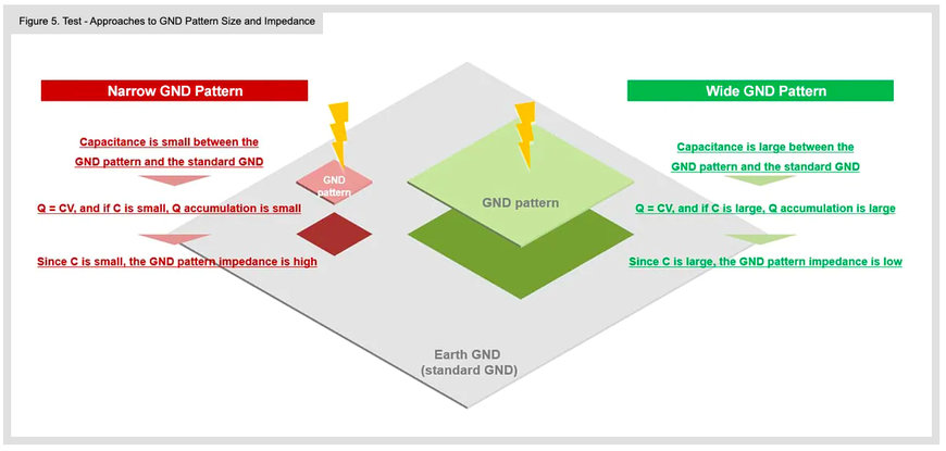
Test - Approaches to GND Pattern Size and Impedance
Test - Improved ESD Countermeasure Methods
When the GND pattern is narrow and ESD suppression effects cannot be obtained from chip varistors, chip varistor ESD suppression effects can be obtained by connecting the GND pattern to the metal body.
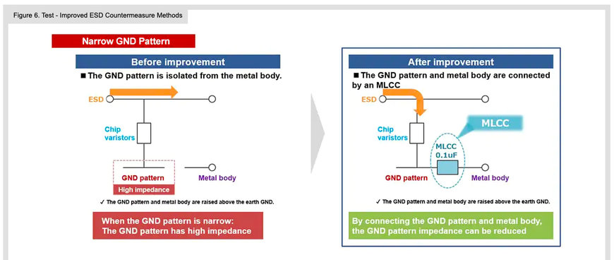
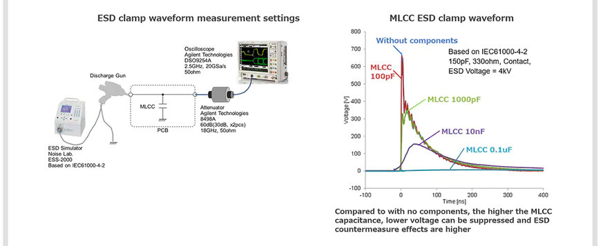
MLCC effects: A 0.1 uF MLCC exhibits low impedance characteristics to ESD, and as a result, low impedance is obtained throughout the entire GND pattern (including the metal body via the MLCC) by connecting the GND pattern to the metal body by an MLCC. As a result, the ESD is bypassed to the GND pattern (including the metal body via the MLCC) through the chip varistor regardless of the size of the GND pattern.
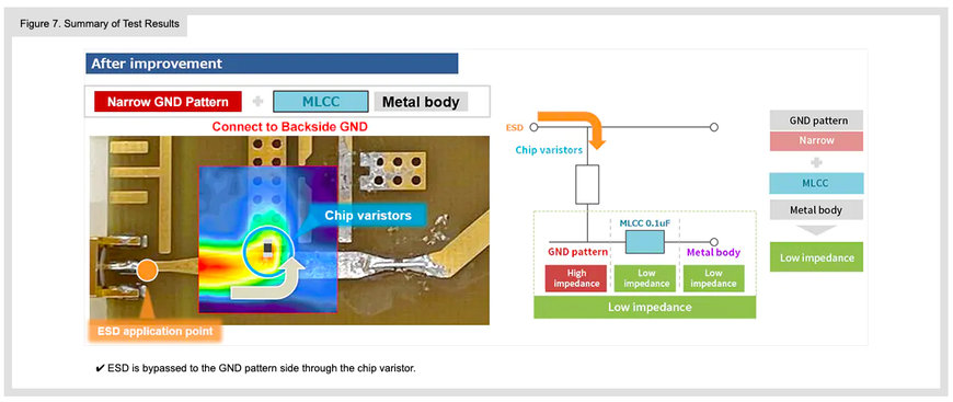
Summary of Test Results
ESD countermeasures when the GND pattern is floating from the metal body or Earth GND
In compact electronic devices and mobile devices, designs where the circuit GND pattern is isolated from the metal body and the earth GND are commonly seen. Even in these cases, the performance of ESD protection components such as chip varistors can be exhibited by making the circuit GND pattern as wide as possible.
If the GND pattern cannot be made wide, there are cases where the ESD suppression effects of ESD protection components cannot be obtained, and the risk of ESD intrusion into circuits increases. By reviewing the design of the device body and the GND pattern circuits, however, performance by ESD protection components can be exhibited. By adopting a circuit design that reduces the impedance of the GND pattern that bypasses the ESD through ESD protection components, a more effective ESD countermeasure circuit can be achieved.
Debugging ESD Problems
When measuring ESD behavior in a signal line using an oscilloscope and attenuator
Under the same settings as Test 1, ESD behavior is confirmed using an oscilloscope and attenuator, rather than ESD visualization equipment.
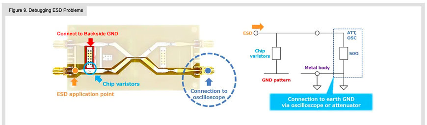
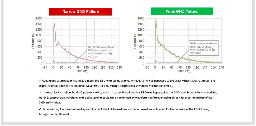
When debugging ESD problems, if a probe or attenuator is connected to check the waveform, there may be an impact on the ESD route from the measurement system, so caution must be exercised. The ESD visualization equipment can take non-connect measurements without the need for probes or other connections.
ESD Technical Support
TDK makes it possible to measure ESD using ESD visualization equipment. If you are having issues with ESD or noise countermeasures, contact TDK for support.
www.tdk.com
