
electronics-journal.com
22
'22
Written on Modified on
Murata Is Seeking Partners to begin discussions for a New Transparent and Bendable Conductive Film along with the Application of New Ideas to Open up the IoT Era (Technical Explanation)
Murata Manufacturing is now developing a new material with unprecedented strong points. This new material combines transparency, flexibility, conductivity, and safety. Furthermore, it realizes high workability to be able to easily draw circuit patterns and other elements with diverse methods.

It is possible that we will be able to create new value with approaches different from conventional technologies for electrical and electronic devices by applying this new material. Murata is seeking partners to discuss with us the application of new ideas using this new material regardless of your business or industry. In this article, which is split into two parts, a technical explanation and the application image, we introduce the strong points of this new material we are developing and the possibilities of its application as envisioned by Murata currently.
There are many examples of the invention of new materials in the background to the development of humankind up to now. The shift from stone tools made with natural materials as they were to earthenware made with ceramics of baked and hardened soil led to the transition from primitive times to the age of civilization.
After that, the invention of bronze and iron gave birth to powerful nations. The invention of semiconductors then built the modern information society. In addition to these major milestones, there are countless other examples of new tools and devices being created from the arrival of new materials. New materials are the source of innovation. The appearance of a new material can be called an event that foreshadows the creation of new value and a new era.
(From left) Naruse, in charge of processing technology development, and Koyanagi, in charge of materials development
Taking on the Challenge of Developing a New Material That Will Contribute to the Creation of Innovation in the Future
The utilization of new materials has also played an important role in the history of the development of Murata's electronic components business. We have developed a capacitor using barium titanate, which is a new material with a high dielectric constant that we developed with the cooperation of (then) Assistant Professor Tetsuro Tanaka of Kyoto University.
This capacitor enabled an increase in capacity while remaining compact. That became the source of the power that supported the expansion in the application and downsizing of electrical and electronic devices after that. Since then, we have consistently integrated the development of materials, processes, and devices to enable the progress of sustainable technologies and the growth of business.
Murata is now taking on the challenge of the development of a new material and its practical use, which will become the source of innovation creation to open up a new era. Koyanagi, who is involved in the development of this material, has the following to say: "Given the characteristics of the new material we are developing, I feel it will be possible to apply it to a wide range of applications beyond just electronic components. For example, I feel it will be possible to apply it to automobiles, industrial machinery, medical, and health-care devices, and also entertainment and sports." This is challenging material development to open up new applications that go beyond the boundaries of conventional business for Murata.
We are unable to clarify the details of the composition and structure of the new material we are developing at the present time. Nevertheless, we would like to focus on some of the new material's features to introduce its possibilities under the name of Transparent and Bendable Conductive Film.
Combines a High Level of Transparency, Flexibility, Conductivity, and Safety
There are broadly two strong points to Transparent and Bendable Conductive Film: it enhances the functions and performance in applications and it produces usage benefits to user companies that develop and produce products to which this material is applied (Fig. 1). We would like to introduce each of these strong points in a little more detail. After that, we will briefly touch on the features and characteristics of Transparent and Bendable Conductive Film as a material.
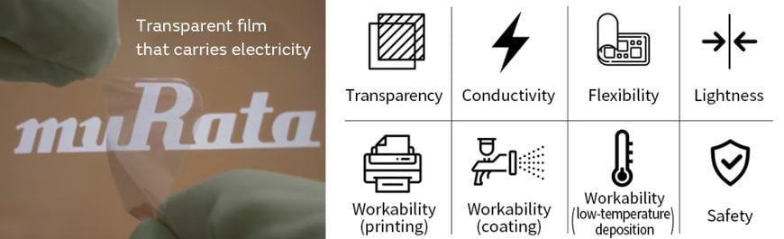
Fig. 1: Transparent and Bendable Conductive Film Developed by Murata and Its Strong Points
First, we will showcase the benefits the new material gives to applied products. As its name suggests, Transparent and Bendable Conductive Film combines conductivity while being transparent. It also has the strong point of not losing those characteristics even when it is bent.
Similarly, conductive films of indium tin oxide (ITO)-based materials used in touch-panel electrodes, wiring, and other components and conductive films using graphene composite material ink serve as transparent and bendable conductive films. If we focus only on individual characteristics such as transparency, flexibility, and conductivity, there are many materials that display even better characteristics. There are also materials that combine two out of three of these strong points. However, it is not easy to find materials that combine these three strong points at a high level like with Transparent and Bendable Conductive Film.
In general, there is a trade-off between transparency and conductivity in transparent conductive films. Transparent and Bendable Conductive Film also follows this. Nevertheless, let's compare its characteristics with those of other materials. Doing so, we find that its sheet resistance* is lower by approximately two digits (approximately a two-digit improvement in conductivity) compared with the ink of graphene composite materials with a similar level of light transmittance (Fig. 2).
On the other hand, if we compare it with a material coated on polyethylene terephthalate (PET) film (a material with relatively bendy characteristics among numerous ITO-based materials), we are already now able to achieve characteristics at the same level or only slightly below that. Moreover, Transparent and Bendable Conductive Film is in the initial stage of development. "Its current characteristics have room for further improvement in the future" (Koyanagi).
*Sheet resistance refers to the electrical resistance of thin film or film-like substances with a certain level of thickness.
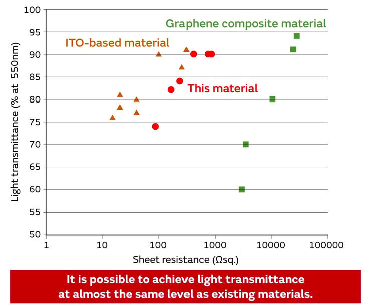
Fig. 2: Measured Values of Sheet Resistance and Light Transmittance for Transparent and Bendable Conductive Film and Existing Transparent Conductive Films
Furthermore, the strong point of this material that it does not lose its characteristics even if bent is superior to the extent that it outperforms graphene composite materials and ITO-based materials (Fig. 3). Even if you repeatedly bend Transparent and Bendable Conductive Film so that it leaves a clear crease after applying it to a substrate, its resistance value does not change.
The wiring cracks and disconnects when it is bent in the case of metal materials used in normal wiring materials. Moreover, the material of existing transparent conductive films itself is hard. Therefore, while it can withstand bending to a certain extent, it will crack if bent to the extent that it leaves a crease. The excellent flexibility of Transparent and Bendable Conductive Film can also be called an extremely unique property applicable to applications for which mechanical loads are constantly applied.
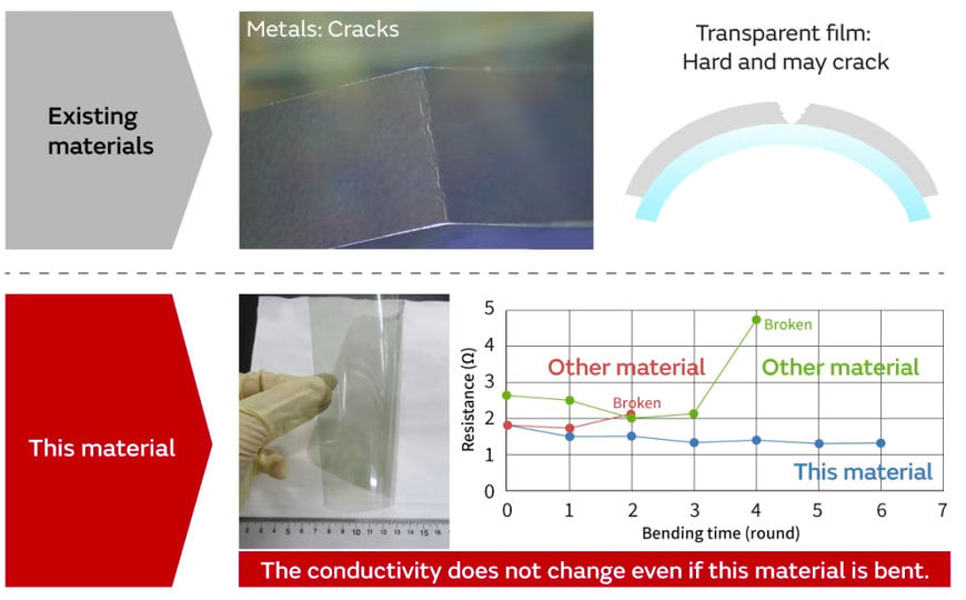
Fig. 3: Comparison of the Bending Resistance of Transparent and Bendable Conductive Film and Existing Conductive Films
Furthermore, Transparent and Bendable Conductive Film is safe, with low skin sensitization, and also has no effect whatsoever even if it comes into contact with a living body. It does not cause metal allergies and does not act as an endocrine disruptor that has various adverse effects on living bodies. Therefore, it is expected to have good compatibility in applying it to biometric information sensing, wearable devices, disposable devices, and other applications.
Excellent Workability That Allows Patterns to Be Drawn as Desired on Substrates of All Shapes
We will look at the benefits this new material will give to user companies that develop and produce applied products here. In general, new materials have strong points not found before. Therefore, they are often difficult to handle in processing systems and other equipment for making existing products. The application of a new material will not spread no matter how excellent its characteristics if it is difficult to use.
Naruse, who is developing technologies that produce an easy-to-use form such as ink based on the Transparent and Bendable Conductive Film material, says the following about this: "It is easy to apply this new material to various applications because it has a high level of compatibility with the coating and processing used in diverse existing processing systems."
Transparent and Bendable Conductive Film is a hydrophilic material. Accordingly, it can be easily and uniformly dispersed in solvents. Therefore, it is possible to produce inks according to the processing method and to use existing coating and printing techniques to form films with stable characteristics. Specifically, it is possible to draw patterns under normal temperatures and pressures with inkjet printers, stamp and screen printing, spray coating, pen drawing, and other methods (Fig. 4). Of course, it will also be possible to open up unknown applications by developing new never-before-seen groundbreaking coating systems and optimizing the ink.
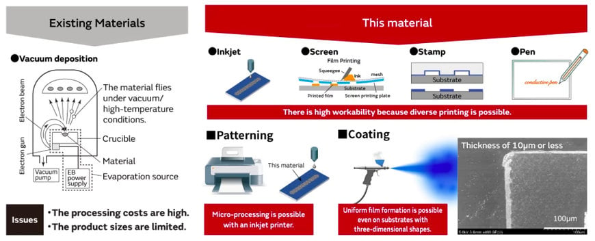
Fig. 4: Possible to Form Wiring Patterns with Various Techniques According to the Needs of the Application
The ability to draw patterns using such diverse processing methods is a strong point that will support expansion of applications. For example, it is possible to draw wiring with fine line widths of several hundred microns by using an inkjet printer. Using such processing methods allows patterns to be drawn as desired without a removal process like masks or etching. In addition, it is possible to draw just the parts that function as conducting wire.
Therefore, it also realizes the effective use of materials and a reduction in the environmental burden. On the other hand, adopting a method of coating with a spray means it is even possible to cover substrates with three-dimensional curved surfaces by using the same method as that of coating the body of an automobile. That enables the formation of conductive film on the surface of large and complex objects. Furthermore, it is also possible to easily add electrical functions to the surface of tools and devices for which the shape itself has meaning.
ITO-based electrodes require some kind of high-temperature treatment to form wiring patterns and similar to exhibit conductivity. For instance, it is necessary to attach film to the substrate with a vacuum deposition process that is performed under a high-temperature and vacuum environment for ITO-based materials. As a result, it has been impossible to avoid an increase in the processing workload and a deterioration of the substrates to be coated. That led to drawbacks including limited applications and increased costs. Transparent and Bendable Conductive Film does not have such factors hindering an expansion in applications.
Another major advantage is the fact that post-processing after the pattern formation is simple (Fig. 5). It is necessary to add a firing process at 150 to 200°C for Ag ink that is one of the conventional materials to form transparent conductive film. This is to ensure conductivity by connecting fine Ag particles to each other after drawing the pattern. Transparent and Bendable Conductive Film can demonstrate conductivity just by drying water at 50 to 100°C. Therefore, it is also possible to form it on substrates vulnerable to heat damage. You can even use it with natural drying if you don't mind waiting for some time.
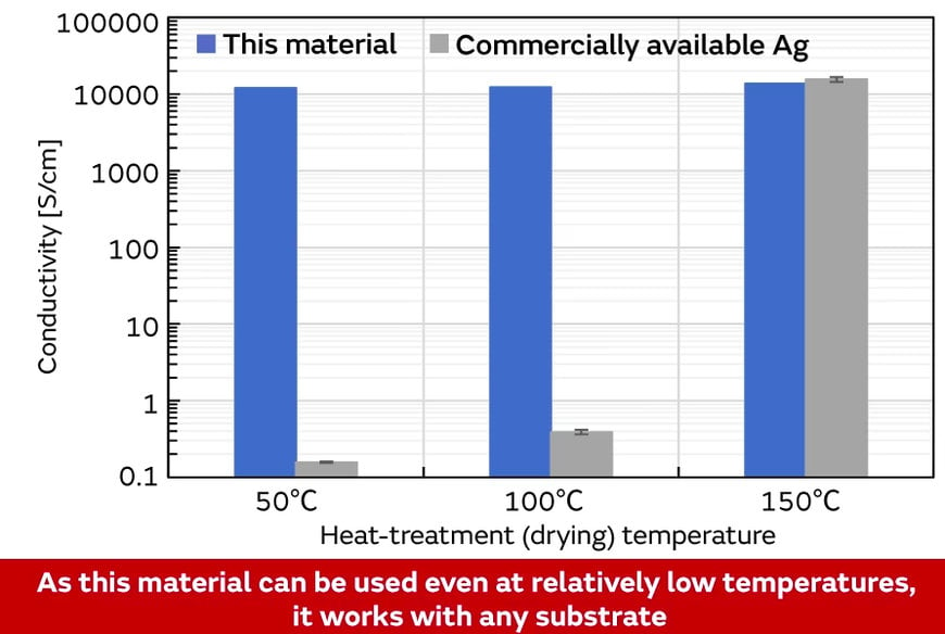
Fig. 5: Transparent and Bendable Conductive Film Manifests Conductivity with Just a Low-temperature Process
Unique Physical Properties Produced by Micro-ceramics
Transparent and Bendable Conductive Film that has all these good points is a material made from micro-ceramics at the nanometer level with the property to carry electricity. The shape of these micro-ceramics is flat. Accordingly, due to the microscopic size and shape of these ceramics, this material exhibits characteristics halfway between metal and ceramics to obtain transparency and conductivity. Its excellent workability is also due to this size and shape. The film after coating and drying the ink in which this material is dispersed enters a state in which the entire pattern drawn is energized because the micro-ceramics lie on top of each other.
Substances have been emerging in recent years that exhibit unique characteristics due to their nano-sized micro-structure and size instead of the composition of their materials like graphene, which demonstrates high conductivity by connecting carbon (C) atoms. Transparent and Bendable Conductive Film can also be called a material that produces unique strong points with the same approach based on ceramics formed from common elements. Production technology is always an issue in achieving the practical use of new materials.
Nevertheless, it is easy to apply the production technologies possessed by Murata. Therefore, this new material also has wonderful mass production performance. Moreover, no rare metals or earths are used. Accordingly, the raw materials are inexpensive and can be stably procured.
In addition, there is room for further adjustments to improve the new material's characteristics and to enhance its suitability for specific applications by optimizing the composition, structure, and size of the micro-ceramics. In other words, it can be called a material with the hidden potential to further evolve and expand its applications in the future. We introduce the way in which electronic and industrial products and related services should be realized with new approaches that Murata has the potential to develop based on Transparent and Bendable Conductive Film at the present time in the Application Image part of this article.
Please tell us your thoughts!We are seeking partners to discuss ideas that will utilize Transparent and Bendable Conductive Film, Click here for details
www.murata.com
