
electronics-journal.com
20
'25
Written on Modified on
Basler Enhances Probe Card Inspection with Advanced Vision & Autofocus Solutions
High-precision vision systems deliver micron-level defect detection, optimized illumination, and integrated autofocus to ensure probe card reliability in advanced wafer testing.
www.baslerweb.com
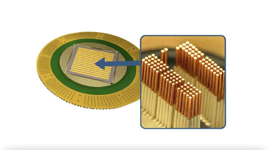
High-density vertical probe card with tightly packed probe arrays for advanced wafer testing
Rising demands on probe card reliability
As device architectures scale toward multi-die packaging and smaller bump pitches, the integrity of every probe tip becomes critical for known-good-die screening. Probe cards used in advanced wafer probing can carry thousands of contacts, and even minor contamination, bending, or wear can compromise test accuracy and reduce yield.
Routine inspection of MEMS and vertical probe cards now requires micron-level imaging across large, reflective probe arrays. Contamination buildup, oxidation, or bent tips must be detected reliably and at high throughput, calling for vision systems that combine advanced illumination, autofocus capability, and powerful algorithms. These solutions provide engineers with consistent, actionable data for probe card QA in demanding 24/7 production environments.
Overcoming vision barriers in probe card defect detection
Different tolerances in XY and Z
Probe card inspection is often labeled a sub-micron task now, but the requirements differ by dimension. In Z direction, coplanarity and overtravel demand sub-micron accuracy, typically handled with 3D metrology.
In contrast, XY pitch and alignment fall within the low-micron range, where advanced 2D imaging excels. Here, the real challenge is not resolution itself, but ensuring stable, repeatable measurements despite reflective surfaces, optical distortion, and variability on the test floor.
Z direction in wafer probe testing requires sub-micron accuracy for tip height, while XY alignment is managed within a few micron tolerance using high-resolution 2D imaging.
Illumination design makes the difference
At fine pitches below 25 µm, probe tips often use tungsten or gold-plated tungsten, while wafer pads are copper or aluminum alloy. These materials create challenging optical conditions: tungsten produces dull metallic glare, gold/nickel plating is highly reflective, and copper pads saturate under coaxial light. Conventional bright-field illumination can hide contamination, scratches, and probe marks within reflections.
Strategic illumination design separates signal from noise. Coaxial light provides even surface definition, dark-field illumination reveals edges and debris, and cross-polarization eliminates specular reflection for stable contrast. Combined with high-magnification telecentric optics and distortion correction, this enables distortion-free imaging for reliable micron-level measurement.
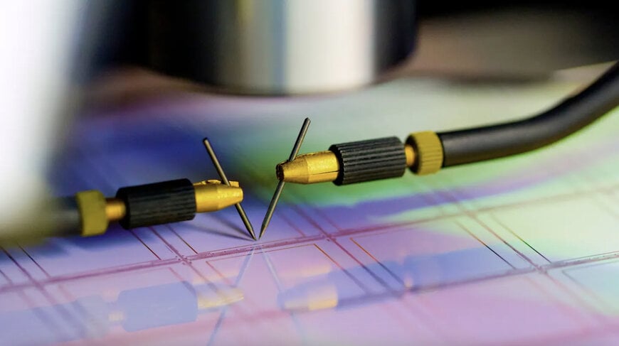
Probe tip defect detection for contamination buildup, oxidation, wear, cracks, and bending that may impact test reliability.
Autofocus keeps probe tips sharp
On large probe cards, variations in tip height and card warpage can push some tips out of the focal plane. Even with optimized illumination, blurred images are difficult to measure accurately. Autofocus technology rapidly adjusts focus during inspection to ensure every probe tip remains sharp and in focus. Basler offers multiple integrated autofocus solutions integrated autofocus solutions, including liquid lens modules from various manufacturers and laser-based autofocus solutions, delivering consistently clear images while maintaining high inspection speeds.
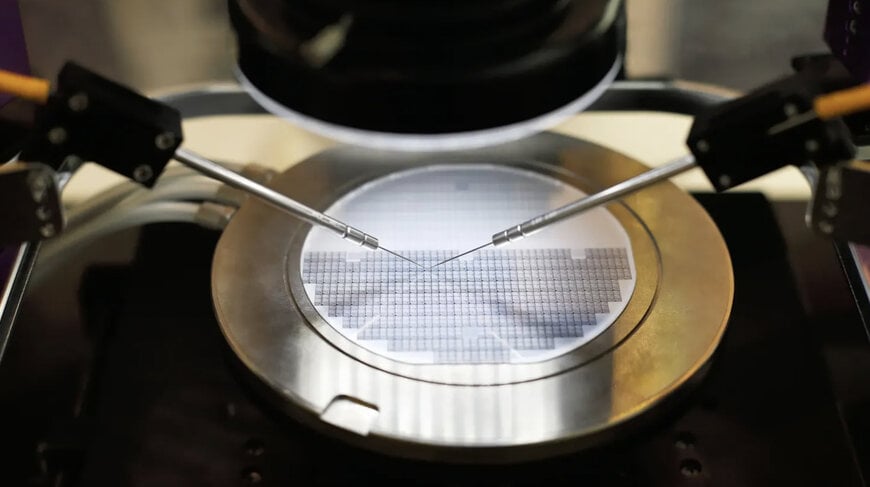
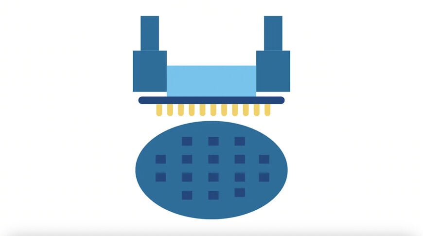
Wafer probe testing powered by vision inspection and alignment
Algorithms that deliver actionable measurements
Once illumination and optics secure a clean image, the next challenge is turning it into usable data.
Typical approaches include Blob Analysis to quantify dirt and debris, sub-pixel edge detection to measure probe width and spacing, and Geometric Measurements to confirm pitch across dense arrays. These are only the starting points on the software part. Engineers also program inspection tasks such as surface texture analysis to distinguish oxidation from contamination.
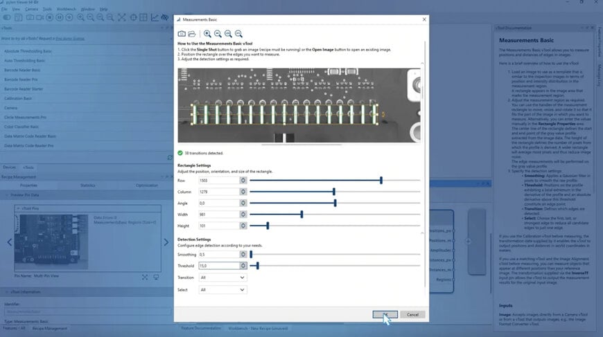
For probe tip QA, algorithms can run efficiently on the PC using Basler’s pylon vTools for measurement and analysis. When higher throughput or multiple cameras increase CPU load, FPGA-based processing with Basler’s VisualApplets and frame grabber ensures real-time performance. Basler supports both paths, combining flexibility with integration-ready performance.
www.baslerweb.com
Rising demands on probe card reliability
As device architectures scale toward multi-die packaging and smaller bump pitches, the integrity of every probe tip becomes critical for known-good-die screening. Probe cards used in advanced wafer probing can carry thousands of contacts, and even minor contamination, bending, or wear can compromise test accuracy and reduce yield.
Routine inspection of MEMS and vertical probe cards now requires micron-level imaging across large, reflective probe arrays. Contamination buildup, oxidation, or bent tips must be detected reliably and at high throughput, calling for vision systems that combine advanced illumination, autofocus capability, and powerful algorithms. These solutions provide engineers with consistent, actionable data for probe card QA in demanding 24/7 production environments.
Overcoming vision barriers in probe card defect detection
Different tolerances in XY and Z
Probe card inspection is often labeled a sub-micron task now, but the requirements differ by dimension. In Z direction, coplanarity and overtravel demand sub-micron accuracy, typically handled with 3D metrology.
In contrast, XY pitch and alignment fall within the low-micron range, where advanced 2D imaging excels. Here, the real challenge is not resolution itself, but ensuring stable, repeatable measurements despite reflective surfaces, optical distortion, and variability on the test floor.
Z direction in wafer probe testing requires sub-micron accuracy for tip height, while XY alignment is managed within a few micron tolerance using high-resolution 2D imaging.
Illumination design makes the difference
At fine pitches below 25 µm, probe tips often use tungsten or gold-plated tungsten, while wafer pads are copper or aluminum alloy. These materials create challenging optical conditions: tungsten produces dull metallic glare, gold/nickel plating is highly reflective, and copper pads saturate under coaxial light. Conventional bright-field illumination can hide contamination, scratches, and probe marks within reflections.
Strategic illumination design separates signal from noise. Coaxial light provides even surface definition, dark-field illumination reveals edges and debris, and cross-polarization eliminates specular reflection for stable contrast. Combined with high-magnification telecentric optics and distortion correction, this enables distortion-free imaging for reliable micron-level measurement.
Probe tip defect detection for contamination buildup, oxidation, wear, cracks, and bending that may impact test reliability.
Autofocus keeps probe tips sharp
On large probe cards, variations in tip height and card warpage can push some tips out of the focal plane. Even with optimized illumination, blurred images are difficult to measure accurately. Autofocus technology rapidly adjusts focus during inspection to ensure every probe tip remains sharp and in focus. Basler offers multiple integrated autofocus solutions integrated autofocus solutions, including liquid lens modules from various manufacturers and laser-based autofocus solutions, delivering consistently clear images while maintaining high inspection speeds.
Wafer probe testing powered by vision inspection and alignment
Algorithms that deliver actionable measurements
Once illumination and optics secure a clean image, the next challenge is turning it into usable data.
Typical approaches include Blob Analysis to quantify dirt and debris, sub-pixel edge detection to measure probe width and spacing, and Geometric Measurements to confirm pitch across dense arrays. These are only the starting points on the software part. Engineers also program inspection tasks such as surface texture analysis to distinguish oxidation from contamination.
For probe tip QA, algorithms can run efficiently on the PC using Basler’s pylon vTools for measurement and analysis. When higher throughput or multiple cameras increase CPU load, FPGA-based processing with Basler’s VisualApplets and frame grabber ensures real-time performance. Basler supports both paths, combining flexibility with integration-ready performance.
www.baslerweb.com
