
electronics-journal.com
23
'26
Written on Modified on
Advanced Electronic Design Automation and Intellectual Property Integration for Next-Generation Process Nodes
Synopsys has expanded its collaboration with TSMC to provide AI-enhanced design flows and silicon-proven interface IP for A14, A16, and 2nm process technologies.
www.synopsys.com
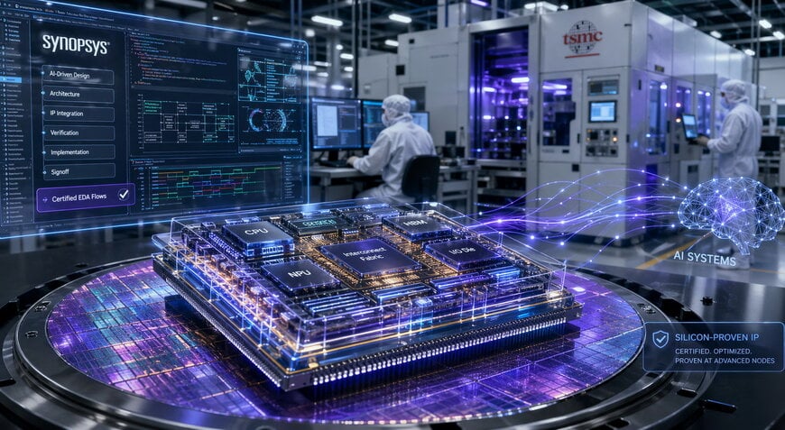
The development of high-performance computing (HPC) and autonomous systems requires sophisticated integration between electronic design automation (EDA) tools and the underlying semiconductor manufacturing processes. Synopsys has updated its portfolio to support TSMC’s most advanced nodes, including the A16 with Super Power Rail and the A14 process. These advancements address the specific physical and electrical challenges of sub-2nm geometries, focusing on improving the quality of results (QoR) through AI-driven optimization and comprehensive multiphysics signoff.
Multiphysics Integration in the Automotive Data Ecosystem
As the automotive data ecosystem shifts toward centralized compute architectures, the demand for high-reliability chiplets has increased. Synopsys has introduced a UCIe IP solution with ASIL B functional safety certification on the TSMC N5A node. This integration supports the automotive industry's transition to modular System-on-Chip (SoC) designs, where components from different vendors must maintain signal integrity and thermal stability under rigorous operating conditions. By providing silicon-proven foundation IP on specialty nodes like N5A and N3A, the collaboration ensures that automotive manufacturers can utilize advanced logic libraries and embedded memories that meet AEC-Q100 standards.
3D Multi-Die Design and Co-Packaged Optics
To mitigate the physical limitations of monolithic chips, the industry is increasingly adopting 3D multi-die architectures. Support for TSMC 3DFabric technologies, such as System on Integrated Chips (TSMC-SoIC) and Chip on Wafer on Substrate (CoWoS), is now integrated into the Synopsys 3DIC Compiler. This unified platform automates the design process from initial exploration to final signoff, utilizing GPU acceleration to reduce the computational time required for thermal and power analysis.
The complexity of a modern digital supply chain requires advanced connectivity solutions. Significant progress has been made in co-packaged optics (CPO) to support high-bandwidth data center requirements. The integration of optical path simulation and photonic device simulation tools allows engineers to model the transition between optical and electrical domains. This is particularly relevant for the newly introduced 224G IP solution, which facilitates Ethernet and UALink connectivity in next-generation electro-optical systems.
AI-Powered Productivity and Physical Verification
The introduction of agentic run assistance within the Fusion Compiler represents a shift toward autonomous design optimization. By utilizing the NanoFlex Pro architecture on the A14 process, the tool identifies timing improvement opportunities throughout the design flow without manual intervention. Furthermore, AI-assisted physical verification in the IC Validator platform targets the acceleration of Design Rule Check (DRC) resolution. These mechanisms are designed to shorten the time-to-market for complex AI accelerators and mobile network processors by reducing the iteration cycles between design and tapeout.
Performance Benchmarks and Interface Standards
The technical roadmap includes several first-silicon milestones across N5, N3P, and N2P processes. The expanded IP portfolio supports established and emerging industry standards:
- Data Interconnect: PCIe 7.0, UCIe 64G, M-PHY v6.0
- Memory Interfaces: HBM4, DDR5 MRDIMM Gen2, LPDDR6
- Process Nodes: A14, A16 (Super Power Rail), N2, N3P
These standards provide the necessary bandwidth and power efficiency for hyperscale data centers. For instance, the inclusion of HBM4 support is critical for memory-intensive AI workloads, providing the necessary throughput to match the processing capabilities of 2nm-class silicon. High-capacity analog power integrity signoff tools have also been scaled to handle the increased transistor density of large N2-based designs, ensuring stable power delivery across the die.
Edited by Evgeny Churilov, Induportals Media - Adapted by AI.
www.synopsys.com
Edited by Evgeny Churilov, Induportals Media - Adapted by AI.
www.synopsys.com
