
PECVD SiCN system for advanced semiconductor processing
ACM Research deploys PECVD SiCN platform to enable BEOL and advanced packaging process control in collaboration with a semiconductor manufacturer.
bodewellgroup.com
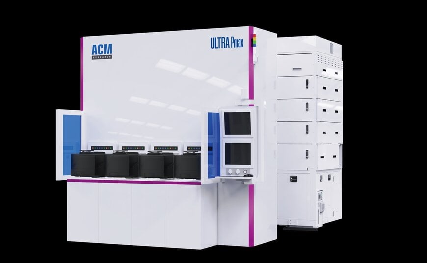
ACM Research has delivered a plasma-enhanced chemical vapor deposition (PECVD) silicon carbonitride (SiCN) system designed for back-end-of-line (BEOL) and advanced packaging applications. The system introduces a multi-station deposition architecture to improve film uniformity, plasma stability, and interface control in sub-55 nm semiconductor manufacturing.
Context and Technical Relevance
Scaling of logic devices below 55 nm increases sensitivity to interface defects, particle contamination, and plasma-induced variability. BEOL processes such as copper interconnect formation require diffusion barriers and etch stop layers with tightly controlled thickness and composition. SiCN films are used in these roles due to their dielectric properties, adhesion characteristics, and resistance to metal ion diffusion.
Conventional PECVD systems typically rely on single-station deposition, limiting control over intra-wafer uniformity and plasma distribution. ACM Research developed a new system architecture to address these constraints in high-density integration environments.
Deposition Architecture and Process Control
The PECVD SiCN system is based on a three-station rotating deposition configuration within a single reaction chamber. Each station deposits approximately one-third of the total film thickness. This segmented approach enables:
- Controlled interface formation between deposition steps
- Stabilized gas flow dynamics across the wafer surface
- Reduced variation in film thickness and composition
Each station operates with an independent radio frequency (RF) plasma source under the “One Station, One RF” control scheme. This allows localized adjustment of plasma power, enabling consistent ion energy distribution and improved process repeatability.
The combination of rotational sequencing and independent RF control supports tighter process windows, particularly for thin-film stacks where deviations in nanometer-scale layers affect electrical performance.
Deployment and Validation
The system was validated against customer-defined process specifications at ACM Research’s Lingang laboratory before shipment. Validation parameters included film uniformity, adhesion strength, and plasma stability under BEOL-compatible conditions.
The equipment has been installed at a semiconductor manufacturing site for further process qualification. Integration involves compatibility with existing wafer handling systems and alignment with established fabrication workflows.
Application Areas and Use Cases
The system is designed for:
- Copper oxidation reduction processes
- Copper diffusion barrier layer deposition
- Etch stop layer formation in multilayer interconnects
- Wafer-level bonding in advanced packaging
In advanced packaging, SiCN films contribute to bonding integrity due to their high density and adhesion energy. These properties support heterogeneous integration and increased interconnect density.
Expected Impact
The multi-station PECVD approach improves process stability by distributing deposition steps and isolating plasma control variables. This reduces defect density and enhances reproducibility across wafers.
For advanced semiconductor manufacturing, the system supports tighter tolerance control required for scaling and complex device architectures. In packaging applications, improved film characteristics contribute to long-term reliability and reduced risk of interconnect failure.
Edited by an industrial journalist, Lekshman Ramdas, with AI assistance.
www.bodewellgroup.com
