
electronics-journal.com
26
'26
Written on Modified on
Heterogeneous Adaptive System-on-Chip Architectures Integrate Standardized Chiplet Interconnects
AMD introduces native Universal Chiplet Interconnect Express support to modularize heterogeneous compute and radio frequency processing within unified multichip packages.
www.amd.com
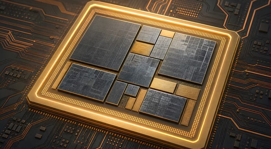
Modular semiconductor packaging increasingly replaces large monolithic dies in aerospace, defense, telecommunications, and high-performance computing to handle escalating routing complexity and thermal dissipation. Integrating the Universal Chiplet Interconnect Express (UCIe) 1.1 standard directly into adaptive system-on-chip (SoC) architectures establishes a low-latency, vendor-agnostic bus across co-packaged silicon.
Die-to-Die Interconnect Architecture and Bandwidth Scaling
Transitioning from board-level high-speed serial interfaces to in-package die-to-die physical layers reduces parasitic capacitance, insertion loss, and power consumption. The implementation of UCIe 1.1 within adaptive computing platforms provides physical layer connectivity supporting up to four independent UCIe standard-package (UCIe-SP) links and up to two UCIe advanced-package (UCIe-AP) links. This dual-topology support achieves aggregate in-package bandwidth in the multi-terabit per second range, eliminating the data transfer bottlenecks previously imposed by serialized printed circuit board traces.
Heterogeneous Compute and Radio Frequency Integration
Radio frequency (RF) front-end applications, optical co-packaged networking, and artificial intelligence acceleration benefit from co-locating disparate silicon processes. Monolithic designs require fabricating digital compute engines, analog-to-digital converters, and RF circuitry on identical process nodes, forcing architectural compromises.
Dedicated adaptive devices integrate multi-channel RF data converters, programmable logic, hard digital signal processing blocks, and AI processing engines delivering up to 80 TOPS (trillion operations per second) of compute. By coupling this architecture with UCIe-compliant physical layers, designers can interface third-party analog front ends, application-specific integrated circuits (ASICs), central processing units, graphics processors, and co-packaged optical modules within a single multi-chip module. This integration reduces size, weight, power, and cost (SWAP-C) parameters while allowing engineering teams to reuse validated silicon intellectual property across multiple product cycles. Initial production silicon featuring these interfaces is scheduled for deployment in the fourth quarter of 2027.
Additional Context
This section details technical specifications and competitive benchmarking not included in the original product announcement.
The adoption of the open UCIe standard reflects a broader industry migration toward multi-vendor chiplet ecosystems, transitioning away from proprietary interconnect standards such as the Advanced Interface Bus (AIB). Competing semiconductor platforms, including the Altera Agilex 9 Direct RF series, integrate high-speed data converters via advanced multi-die packaging topologies like Embedded Multi-die Interconnect Bridge (EMIB). While earlier generations relied on vendor-specific protocols, the transition of programmable architectures to UCIe 1.1 establishes standard data transfer metrics — such as sub-nanosecond physical layer latencies, power efficiencies under 0.5 picojoules per bit, and shoreline interconnect densities exceeding hundreds of gigabits per second per millimeter — enabling direct interoperability with third-party accelerator and memory chiplets.
Edited by Evgeny Churilov, Induportals Media - Adapted by AI.
www.amd.com
