
electronics-journal.com
14
'26
Written on Modified on
Advanced Packaging Solutions for X-Ray Inspection and Warpage Correction
ZEISS is expanding its semiconductor manufacturing portfolio with new metrology equipment designed to address process control challenges in high-density chiplet architectures.
www.zeiss.com
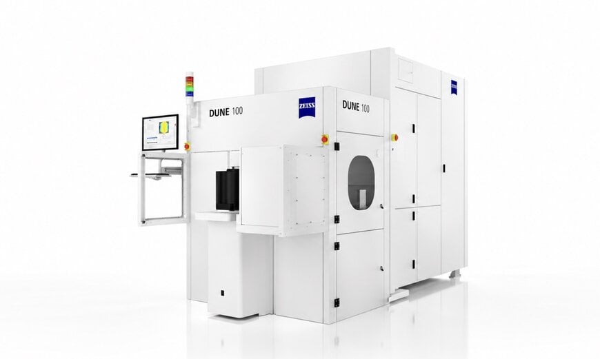
ZEISS Semiconductor Manufacturing Technology is releasing the ZEISS NLX and ZEISS DUNE systems to enhance process control and precision in leading-edge microchip production. These solutions target advanced packaging applications by providing non-destructive internal inspection and active wafer bow correction for 300-millimeter semiconductor wafers.
Non-Destructive Inspection for High-Density Architectures
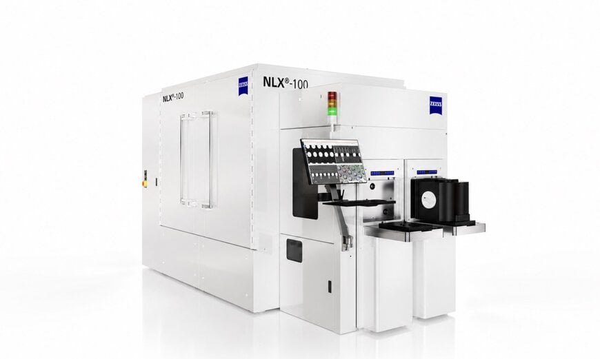
As semiconductor architectures integrate multiple dies into compact spaces, verifying internal structures and connections becomes critical. The ZEISS NLX system enables non-destructive, inline X-ray inspection of complex chip packages. By visualizing the internal structures of 300-millimeter wafers, the system allows manufacturers to inspect connections between stacked dies and detect potential yield-limiting defects early in the production cycle. This capability supports both process development and high-volume manufacturing environments.
Wafer Topography Measurement and Warpage Correction
Thermal and mechanical stresses during complex production steps often induce wafer bow, a geometric deformation that creates challenges in downstream processing and bonding operations. The ZEISS DUNE system addresses this by measuring the topography of individual wafers and applying localized corrections to flatten the substrate. Modifying wafer warpage ensures planar alignment for subsequent lithography or bonding steps, directly mitigating yield losses in advanced packaging workflows.
Christoph Hensche, President of ZEISS Semiconductor Manufacturing Optics, notes that the next generation of semiconductor manufacturing relies on the precise interaction of highly complex process steps, requiring deep expertise in optical systems and process control to bring future chip generations into production reliably at scale.
Photomask Metrology for Extreme Ultraviolet Lithography
At the SEMICON West trade show (October 13–15, 2026), the company highlighted its broader semiconductor manufacturing portfolio, emphasizing photomask solutions critical for stable lithography. The ZEISS AIMS EUV 3.0 system inspects photomasks under optical conditions comparable to those in an extreme ultraviolet (EUV) wafer scanner. This emulation method identifies and evaluates critical defects prior to production exposure. Compatible with both Low-NA and High-NA EUV lithography, the system triples mask throughput compared to previous iterations. For localized defect remediation, the ZEISS MeRiT system provides targeted repair of nanoscale anomalies on photomasks, functioning as a complementary qualification step to the AIMS EUV platform.
Axel Christian, President of ZEISS North America, indicates that as device geometries shrink, early defect evaluation through robust mask solutions becomes increasingly necessary to maintain stable lithography processes.
Additional Context
This section details technical specifications and competitive benchmarking not included in the original news release.
In the inline X-ray inspection market for advanced packaging, the ZEISS NLX competes with automated X-ray inspection (AXI) systems such as the Bruker X-ray metrology tools and the Nordson DAGE series. While traditional AXI systems frequently utilize 2D or 2.5D X-ray imaging optimized for surface-mount technology (SMT) inspection, advanced packaging for 300-millimeter wafers requires high-resolution 3D X-ray microscopy to resolve micro-bumps and through-silicon vias (TSVs) at the sub-micron level. For wafer warpage management, systems like ZEISS DUNE operate in a specialized sector often addressed by optical topography metrology tools from companies like KLA or Onto Innovation. However, direct, active bow correction integrated into the metrology step provides a highly differentiated mechanism compared to standalone measurement tools.
In the EUV photomask inspection domain, the ZEISS AIMS platform operates alongside actinic blank inspection (ABI) and actinic patterned mask inspection (APMI) tools produced by Lasertec. The primary benchmark for actinic inspection is the ability to emulate the exact 13.5-nanometer wavelength of EUV scanners, ensuring that phase defects and multilayer anomalies are detected exactly as they will print on the silicon wafer.
Edited by Aishwarya Mambet, Induportals Editor, with AI assistance.
www.zeiss.com
