
electronics-journal.com
15
'26
Written on Modified on
Scaling Through-Glass Via Metallization for Panel-Level Packaging
VON ARDENNE expands semiconductor deposition to panel-level packaging using high-power impulse magnetron sputtering on its HISS platform to resolve through-glass via metallization limits.
bodewellgroup.com
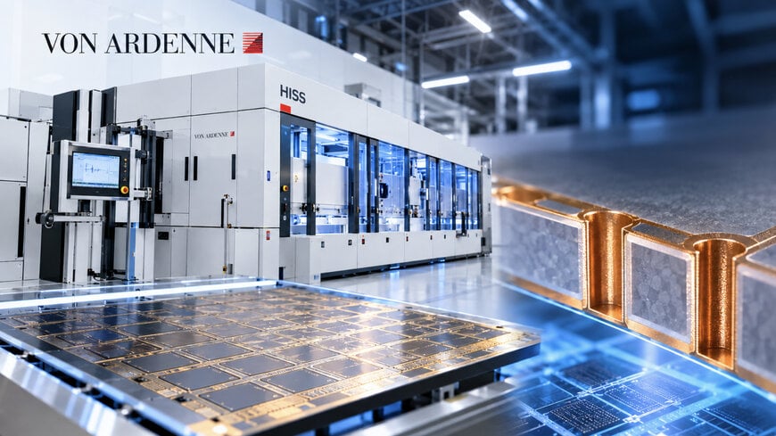
Advanced semiconductor packaging faces severe physical and economic boundaries as high-performance computing and artificial intelligence processors require interposers larger than conventional 300 mm silicon wafers can support. Panel-level packaging addresses this bottleneck by migrating processes to large rectangular glass or organic substrates, yet metallizing high-aspect-ratio microstructures across expansive surface areas introduces severe deposition defects, including overhangs, voids, and poor metal-to-dielectric adhesion. VON ARDENNE has expanded its semiconductor vacuum coating portfolio into panel-level packaging by deploying high-power impulse magnetron sputtering, commonly known as HiPIMS, on its established HISS modular horizontal coating platform.
Operating Mechanism of Ionized Sputtering in High-Aspect-Ratio Structures
The primary engineering challenge in advanced packaging metallization lies in coating through-glass via microstructures and dense redistribution layers without sidewall thinning or pinholes. Standard direct-current magnetron sputtering generates a flux composed mostly of neutral sputtered atoms, which travel in cosine-distributed trajectories that deposit excessively at via openings while starving the sidewalls and bottoms. HiPIMS alters this physical mechanism by applying unipolar pulses of high peak power at low duty cycles.
This pulsed electrical discharge generates ultra-dense plasma exceeding densities of 10 to the power of 18 electrons per cubic meter, ionizing a high fraction of the sputtered metal atoms. When substrate biasing is applied, the ionized target atoms are accelerated perpendicularly into deep via cavities. In through-glass via holes, this directional ionic flux deposits conformal, dense, and highly adherent barrier and copper seed layers, eliminating the premature pinch-off and overhang defects typical of non-ionized physical vapor deposition.
Substrate Transition from Wafer to Large-Scale Horizontal Panel Handling
Scaling physical vapor deposition from round 300 mm silicon wafers to rectangular glass panels requires uniform plasma distribution and mechanical stability over significantly broader surface areas. The integration of HiPIMS onto the modular horizontal HISS platform establishes an industrial-scale manufacturing route that maintains layer uniformity and structural density across panel dimensions.
Dr. Holger Pröhl, head of technology and application at VON ARDENNE, stated that HiPIMS reduces downstream manufacturing costs because enhanced adhesion and denser films minimize rework, extend operational service life, and in specific process flows eliminate intermediate surface-conditioning steps. By mitigating delamination between thin films and smooth glass substrates, manufacturers can improve fabrication yield in demanding semiconductor packaging segments.
Throughput and Economic Drivers in Advanced Heterogeneous Integration
The migration from 300 mm round formats to large rectangular panels maximizes usable substrate area, mitigating the edge-exclusion losses inherent to circular wafer geometries when processing large-area multi-chiplet modules. This dimensional efficiency is central to meeting high volume demands in advanced packaging architectures, including redistribution layer trace formation and 3D stacking.
Market research by Yole Group indicates that panel-level packaging generated more than 300 million dollars in revenue in 2025 and is projected to expand at a compound annual growth rate exceeding 40 percent over the next five years. Market acceleration toward 2029 and 2030 is projected to stem from the entry of major foundries such as TSMC and the rapid adoption of high-density packaging architectures designed for artificial intelligence hardware and high-performance computing, according to Yole Group's March 2026 report titled "Panel Level Packaging 2026".
Guido Ueberreiter, vice president of semiconductor strategy at VON ARDENNE, noted that reliable substrate handling coupled with precise deposition technology serves as a critical enabler for panel-level packaging, providing the process stability necessary to transition established wafer recipes onto large-format panels while maintaining sub-nanometer film performance.
VON ARDENNE presented this deposition technology at SEMICON West 2026, which took place from October 13 to 15 at the Moscone Center in San Francisco.
Additional Context:
This section details technical specifications and competitive benchmarking not included in the original product announcement.
In through-silicon via and through-glass via metallization, the primary technological benchmarks for barrier and seed layer deposition are standard direct-current physical vapor deposition, atomic layer deposition, and chemical vapor deposition. While atomic layer deposition achieves near 100 percent step coverage in high-aspect-ratio holes exceeding 10:1 or 20:1, its chemical precursors yield slow deposition rates, frequently below 0.1 nanometers per second, making it cost-prohibitive for high-throughput panel manufacturing. Conversely, conventional direct-current magnetron sputtering offers fast bulk deposition rates but exhibits poor bottom coverage in vias with aspect ratios above 5:1, leading to asymmetric seed layers that compromise subsequent copper electroplating.
HiPIMS serves as an engineering compromise by ionizing 50 to 90 percent of sputtered atoms, achieving sidewall and bottom coverage comparable to chemical methods while retaining the high film purity, low electrical resistivity, and high throughput of physical vapor deposition. In through-glass via processing, smooth glass surfaces typically exhibit poor mechanical interlocking with sputtered copper, resulting in adhesion strengths below 5 megapascals and frequent film delamination during thermal cycling. The high kinetic energy of ions in HiPIMS creates an atomic intermixing layer at the interface, significantly enhancing adhesion strength and preventing micro-cracking caused by coefficient of thermal expansion mismatches between copper and glass cores.
Edited by Sucithra Mani, Induportals editor – adapted by AI.
www.bodewellgroup.com
