
electronics-journal.com
15
'26
Written on Modified on
Computational Lithography Workflows in Semiconductor Manufacturing
Siemens and NVIDIA integrated the cuLitho CUDA-X library into Calibre software to solve advanced patterning runtime bottlenecks for leading-edge nodes.
www.siemens.com
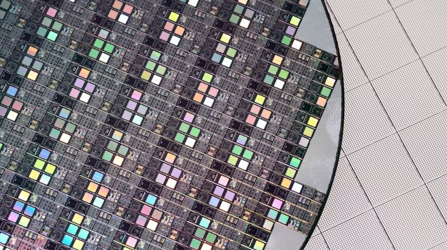
Siemens and NVIDIA Corporation expanded their technical collaboration to integrate GPU-accelerated computing into semiconductor manufacturing flows. The technical architecture embeds software libraries directly into physical verification pipelines to accelerate numerical simulations across high-numerical-aperture extreme ultraviolet lithography environments.
Semiconductor Patterning Bottlenecks and High-NA Challenges
Leading-edge process nodes require advanced optical proximity correction and curvilinear inverse lithography technology to project circuit geometries onto silicon wafers accurately. As critical dimensions shrink, traditional central processing unit clusters encounter computational limits when resolving wave optics equations and diffraction effects at full-chip scale.
Without accelerated computing architectures, engineering teams often compromise optimization depth to maintain tapeout schedules. These constraints heighten the probability of lithographic hotspots, narrow process windows, and lower wafer yield in artificial intelligence processors and memory hardware.
Architecture Integration and Partner Responsibilities
To resolve these computational limitations, Siemens integrated the NVIDIA cuLitho software library with its Calibre manufacturing platform. Within this architecture, NVIDIA develops and maintains the underlying CUDA-X acceleration libraries designed to execute complex mathematical transforms on graphics processing units. Siemens connects these routines directly into signoff-grade Calibre algorithms, maintaining baseline algorithmic accuracy while shifting vector-intensive arithmetic to parallelized hardware.
The integrated software pipeline processes curvilinear mask geometries and electromagnetic field simulations simultaneously. This division of engineering roles enables semiconductor foundries and photomask manufacturers to deploy full-chip inverse lithography workflows without disrupting established electronic design automation environments.
Operational Performance and Industrial Verification
Verified engineering data demonstrates acceleration factors ranging between 10x and 17x across critical computational lithography workloads compared to conventional execution environments.
“Computational lithography has traditionally been one of the most compute-intensive stages of the design-to-manufacturing flow,” stated Ankur Gupta, executive vice president, EDA IC Portfolio, Siemens. “By combining Siemens’ signoff-grade Calibre technology with NVIDIA’s GPU acceleration, we are giving our customers the ability to deploy advanced patterning strategies like curvilinear ILT at scale.”
“By bringing NVIDIA cuLitho acceleration to Siemens’ Calibre, we’re enabling engineers to tackle increasingly intricate patterns and explore more extensive optimizations needed to manufacture the world’s most advanced chips,” stated Tim Costa, vice president and general manager of industrial and computational engineering at NVIDIA.
Production Impact on Mask Synthesis and Process Windows
The reduction in calculation runtime expands process margins by allowing multiple simulation iterations within standard manufacturing schedules. Mask synthesis teams can identify physical defects and optical hotspots prior to physical mask fabrication, improving exposure latitude across High-NA EUV scanners. The increased computational capacity allows continuous deployment of curvilinear patterns, establishing deterministic defect reduction mechanisms for advanced semiconductor nodes.
Edited by Evgeny Churilov, Induportals Media - Adapted by AI.
www.siemens.com
