
electronics-journal.com
24
'20
Written on Modified on
Graphene – then, now and in the future
John Tingay, CTO, Paragraf
Disruptive technology doesn't come along every day, so it's not surprising that when two-dimensional materials started to emerge, they made quite an impact. The most impactful was probably graphene, the story of which crossed over to the popular media like few discoveries. Meeting the expectations of the hype this generated was always going to be difficult, but if it was easy, everyone would be doing it.
This carbon-based material, which is only one atom thick (hence the name, two-dimensional material) has many amazing properties but in the world of integrated electronics, the most significant are probably its high electrical and thermal conductivity. These two, largely interrelated properties play a big role in the performance of semiconductor components. With the continued drive for higher efficiency, it's not surprising that graphene was expected to revolutionise the industry. It has been a long road, but with the introduction of Paragraf's first commercial product, a Hall effect sensor that out-performs all round any other comparable sensor available today, the momentum is building.
Part of the reason for the long gap between researchers isolating graphene in 2004 and being able to use it in production relates to the way it is made. The first examples were isolated by pulling the atoms off a graphite block using sticky tape; clearly this is not very scalable or reliable.
Many methods have been explored since then, including taking blocks of carbon and pulverising them into nanoparticles. Another technique, called liquid phase epitaxy, involves using evaporating or reacting liquids to form a film or platelet on a surface and then removing it. Sublimation is a method that involves thermally reducing a solid that contains carbon until only the carbon is left.
Exposing gases that contain carbon to high temperatures will cause the gas to deposit its carbon on a surface. This process, called chemical vapor deposition, is similar to the process used to deposit materials in semiconductor manufacturing processes. When the high temperatures needed for this process are generated using a plasma source, it is called plasma enhanced chemical vapor deposition, or PE-CVD.
Today, graphene is available in various forms, based on the method used to create or separate it. This makes it much more usable, such as an additive to other materials to increase their robustness or strength. As an example, paint with added graphene is now used on ships to reduce water friction. Carbon composite materials are now also used in aircraft wings.
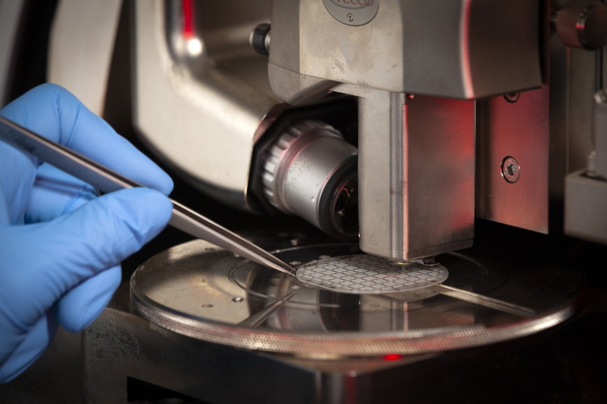
In semiconductor electronic fabrication the methods used are almost exclusively based on CVD; mastering this process is fundamental to the future of graphene in the semiconductor industry. However, there are still challenges to overcome. As anyone who has ever seen inside a semiconductor wafer processing plant knows, the need for purity and cleanliness is paramount to achieving high yields. The process used by most graphene companies targeting the semiconductor industry uses CVD to deposit a carbon-based material on a catalyst, typically copper or nickel, rather than directly onto the semiconductor wafer. This then means the catalyst material needs to be etched away to leave the graphene and the graphene transferred to a second substrate. It is a complex process that is prone to contamination, which is counterproductive to the semiconductor process.
The proprietary technique developed by Paragraf addresses this challenge, as it allows the graphene to be deposited and formed directly onto the semiconductor substrate. This results in a one-atom thick layer that is completely free from contaminants. It is this technique that Paragraf has used to manufacture its first product, the Hall effect sensor. Because graphene has a very low sheet carrier concentration, this results in a sensor that is extremely sensitive to magnetic fields; as a result, the Graphene Hall Sensor (GHS) is as much as 30 times more sensitive than a Hall effect sensor manufactured using conventional semiconductor technology.
Another major benefit of the manufacturing process perfected by Paragraf, which is based on Metalorganic Chemical Vapor Deposition, or MOCVD, is its flexibility. This means Paragraf can tune it for various applications, as well as create stacked monolayers to make it useful in other types of semiconductor devices.
The production of the GHS is now underway at Paragraf's manufacturing site, with the Magnetics Lab at CERN as one of the early collaborators. Because the basic equipment and base wafers are sourced directly from the semiconductor manufacturing supply chain, Paragraf will face no challenges in scaling up production in the future. Longer term, the option to partner with larger semiconductor device manufacturers is also viable.
In all the ways that can be measured today, graphene is a wonder material. Paragraf has made a significant breakthrough in its scalable manufacturing. When applied to semiconductor manufacturing it means graphene can once again be holding great promise.
www.paragraf.com
