electronics-journal.com
07
'21
Written on Modified on
Reinventing Chip Design from the Outside In
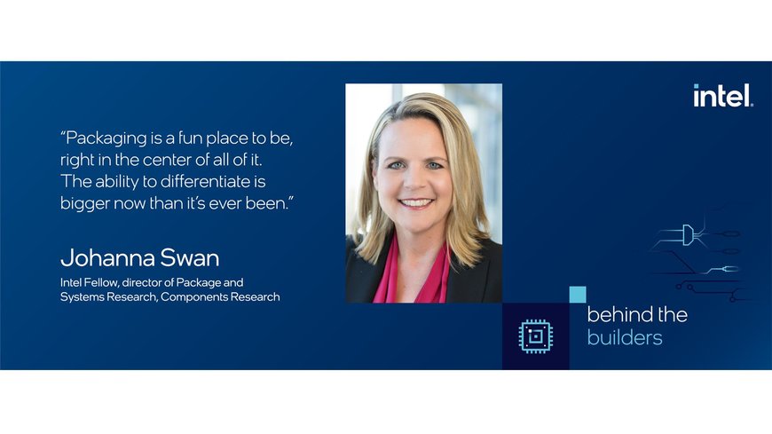
In the first ‘Behind the Builders,’ Intel Fellow Johanna Swan explains how chip packaging went from a basic utility to ‘a real inflection point, maximizing performance per volume.’

In describing Intel’s foray into customer chipmaking through Intel Foundry Services and how it stands apart, Intel CEO Pat Gelsinger has repeatedly cited “our world-class packaging and assembly test technologies.” Gelsinger told investors last month that “we are seeing extreme interest in our packaging technologies” from potential foundry customers.
Packaging has never seen so much love.
But for Johanna Swan, deferred adoration goes with the job. As director of Package and Systems Research in Intel’s Components Research group, Swan says, “We have to anticipate what the future demands are and get focused on what we believe is going to have value — but it’s going to be five years-plus out.”
An Intel Fellow, Swan is an expert in electronics packaging technologies who came to Intel in 2000 after 16 years at Lawrence Livermore National Laboratory.
Swan and her team improve and invent new ways that silicon chips get dressed for work — not only for potential foundry customers but also the wide span of leadership products from Intel. By definition, the package is the enclosure around one or many silicon die that protects them from the outside world, removes heat, delivers power and connects them to the rest of the computer.
“Packaging is there to make external connections,” Swan explains, “but at the same time optimize the performance of what’s going on inside, all the way down to the transistor level.”
Doing research on the far edge means “you have to be super persistent,” she says. “It takes a long time to see your work in the product, so you have to be happy with solving interesting problems and having faith and confidence that it will have an impact and make a difference.”
To call Intel’s packaging-fueled evolution in chip design and manufacturing “a difference” would be an understatement.
A New Inflection Point in the Moore’s Law Quest
“We’re moving from doing everything monolithically to finding ways to create products with multiple nodes, different silicon processes — and get the biggest bang for the buck out of each of those process nodes for their application,” Swan explains.
The ability to put many separate silicon tiles together through assembly, she adds, is “a real big inflection point … an enabler to effectively continue Moore's Law in a slightly different way.”
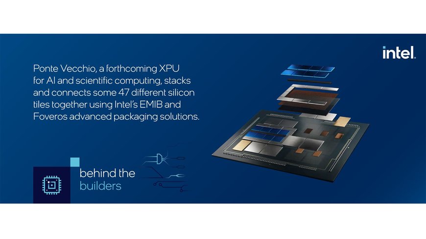
The traditional cornerstones of packaging — performance, cost and manufacturability — carry on, Johanna explains. But the availability of new multidimensional advanced packaging technologies like Intel’s embedded multi-die interconnect bridge (EMIB) and Foveros are giving chip architects “these interesting knobs to optimize and create a system.”
The current paragon of this novel approach is Ponte Vecchio, a forthcoming XPU that stacks and connects some 47 different silicon tiles together to deliver a new order of magnitude in performance for artificial intelligence and scientific computing.

‘What’s So Cool about Packaging’
The next cornerstone of packaging, Johanna explains, is what she calls “functional densification … maximizing the performance per volume.” Though packaging has not had an analog to Moore’s Law, she says, it has advanced in part through miniaturization.
The relative size of the connections and wires (interconnects) in the package versus those found in the silicon die “used to be at drastically different scales,” Swan notes. But as features of packaging technologies shrink — such as die-to-die vertical interconnects reaching pitches well below 10 microns — “the interface is merging between packaging and what Intel calls the very far rear end of silicon.”
“Now all of a sudden, what’s so cool about packaging is it’s at the same feature size as the giant metals on the far back end of a wafer,” says Swan.
That “shifts some of the burden of manufacturing to be in environments that are much more like fabs today,” she adds. But when you look at the total product cost, “we should be able to optimize that in a way that we can actually drive costs down.”
These sophisticated products bring a new set of challenges, Swan says, “but it’s really good for Intel because we already have those strengths.”
That persistent new set of challenges has kept Swan focused on next-generation packaging technologies for two decades and counting. “I thought it would be interesting for a few years, but packaging has many disciplines — high-speed signaling and power delivery and mechanical problems and material challenges. There are a lot of really interesting problems to solve.”
Creating, Pioneering and Disrupting — Thoughtfully
“The ability to create from here has been amazing,” she adds. “I think if you’re curious and you want to solve challenging problems, Intel is a great place and packaging is taking off.”
As far as what’s coming next? That would be secret, but Swan says we always look at today’s bottlenecks and how to improve them, in addition to anticipating changes in both chip design and customer needs.
“Then there’s this other total pioneering area where you start to see a capability that hasn’t really been looked at. You can start to think about how you might do something differently that no one’s really thought of yet.”
“Our charter is to be disruptive,” Swan says. “The art is to make a change without changing all the equipment, without demanding a whole new line. Some of your biggest deltas can still happen by being smart about how you make the disruption.”
“Packaging is a really cool and fun place to be, right in the center of all of it,” she adds. “The ability to differentiate is bigger now than it’s ever been since I came to Intel.”
www.intel.com

