electronics-journal.com
06
'21
Written on Modified on
The Revolutions that Led to Chips Made Like Quilts
‘Behind the Builders:’ Intel Fellow Ravi Mahajan found packaging technologies were improving on a disturbingly straight line, inspiring an approach that was simple in concept but hard to pull off.

For someone who spends most of his work in the future of electronics, Ravi Mahajan finds inspiration in unexpected places: history books.
“If you look at the energy of individuals who drove change,” Mahajan says, “you will see a lot of people who have tried to do things differently — and then coupled opportunity with innovation.”
A voracious reader of history, mathematics, philosophy and big thinkers like Roger Penrose, Mahajan says studiousness was instilled by his mom, a high school principal. He joined Intel after completing his Ph.D. in 1992, and he’s been finding opportunities to innovate ever since.
“I happened to catch the train at the right time,” he says.
Mahajan is an Intel Fellow and director of Pathfinding in the company’s Assembly Test Technology Development group, which figures out new and better recipes to package silicon die. “We are the group that builds the infrastructure” around computer chips, he explains, “bridges between silicon and the real world.”
‘Quiet Revolutions’ in Packaging
Packaging has undergone what Mahajan calls “quiet revolutions” throughout his career, including major changes in materials and design alongside dramatic increases in power (and thus heat to be managed). But recent advances in packaging — particularly those enabling modular design and heterogeneous integration — have put packaging into the spotlight.
Mahajan is partly to blame, too.
As far back as 2007, he says, “some people had figured out that you can’t build bigger and bigger pieces of silicon — you have to disaggregate” to break the chip’s design into smaller separate die and then reconstruct them in a package. “So the question was, how do you take the interconnect in those elements and make it behave like on-silicon interconnect?”
More “Behind the Builders:” Reinventing Chip Design from the Outside In (Johanna Swan)
In other words, how do you eliminate the tradeoffs of breaking chips apart and reassembling them?
Mahajan plotted the historical input/output per millimeter — how many wires connect to a die per layer of a package — “and I saw that it fell on a straight line.” Interconnect density was increasing at a constant and slow rate, roughly 10% per generation. “That bothered me that it was always linear.”
“So I sat down one day and I drew out the core idea for EMIB, and it’s about five to 10 times more dense than what you get on a traditional package.”
EMIB and Foveros Combine for Multidimensional Design
EMIB stands for embedded multi-die interconnect bridge, a simple idea that was hard to pull off. EMIB moves the interconnects into a tiny silicon chip, sized appropriately for the two chips it’s connecting (like a door hinge), that’s then implanted in the package between those two chips.
The bridge chip itself is simple and easy to make as far as silicon chips go — but then it’s thinned to “half the thickness of a sheet of paper,” carefully placed and glued into position and then “bonded with about 8,000 solder joints without goofing up any of them,” Mahajan explains.
He fondly recalls the years spent perfecting all the intricacies as “a pretty interesting experience.” EMIB now is a critical ingredient in millions of Intel chips (thus far, primarily in Intel® Stratix® 10 and Intel® Agilex FPGAs and targeted for servers).
The other breakthrough in packaging technology that Mahajan and team helped bring to fruition is Foveros, which enables two processors stacked vertically to talk to each other using area interconnects (whereas EMIB is a peripheral interconnect, connecting die from edge to edge).
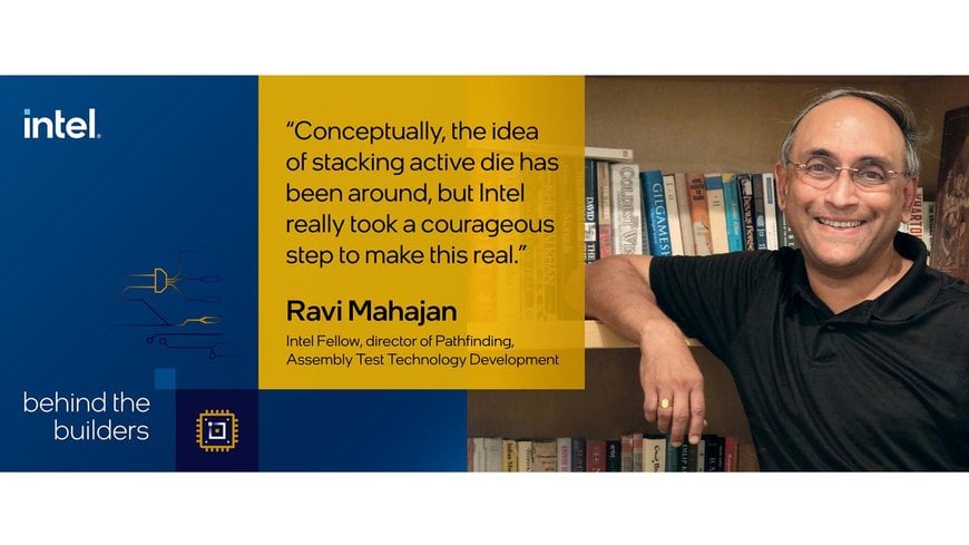
“Conceptually, the idea of stacking active die has been around,” he says, “but Intel really took a courageous step to make this real.”
EMIB and Foveros can also be combined into what Intel calls Co-EMIB, and “now in all three dimensions, you have building blocks that you can stitch, mix and match,” Mahajan explains. “That gives you a tremendous capability in your hands. You can stitch a whole bunch of stuff on the package, each individually optimized, that you could never put on the same piece of silicon.”
These capabilities create a whole new game in chipmaking, expanding from what you can design to what you can mix and match.
Applying Breakthroughs in Chip Packaging to Whole Systems
The next frontier? As Intel continues to improve and invent new ways to put many chips together on “system on packages,” Mahajan sees the emergence of co-packaged photonics as the “potential to change the way computing and communications happen.”
By using light, photonics move data exponentially faster than wires. “If EMIB and Foveros are on-package interconnects, photonics is your off-package interconnect,” Mahajan explains. With new orders of magnitude in chip-to-chip and system-to-system throughput, you could create “clusters of compute and memory, aggregated, disaggregated — whatever ideas people have to architect systems in better ways, we are working on providing them the tools do this.”
“The roadmap has a lot of runway,” Mahajan asserts. And he would know. He represents Intel on IEEE’s Heterogeneous System Roadmap, an industrywide effort to guide the future of mix-and-match chipmaking.
“We are in generation one; we have room to grow up to generation five and more,” he says. “Somebody starting a job now in packaging has got a future for the next 30 years at least.”
That’s plenty more time to apply smart thinking and lessons from toolmaking, food production or other developments through history. “I look for inspiration anywhere I can find it,” Mahajan says.
“Every day is lot of fun,” he adds. “If you want a fruitful engineering career, packaging is very promising right now.”
www.intel.com

