electronics-journal.com
28
'21
Written on Modified on
Back-End Automation and the Future of Semiconductor Manufacturing
Recent events including the pandemic, shipping problems in the Suez Canal, and chip shortages experienced in sectors such as automotive have focused businesses’ attention on strengthening the security of supply chains. In addition, there are ongoing concerns about the environmental effects of international shipping and the benefits of manufacturing locally.

Supply and support for back-end automation is essential to ensure a resilient semiconductor supply chain.
Leading economies are dependent on supplies of semiconductors to power the high-tech innovation that they are hoping will continue to keep them at the forefront of prosperity. It’s no surprise that they are keen to encourage a healthy indigenous semiconductor industry to secure their position and address the concerns over transportation, supply chain, and the environment.
Currently, the semiconductor industry is worth more than $500 billion globally. The EU has signalled its intention to invest in advanced semiconductor technologies to increase the proportion of the world’s semiconductors that is produced in the EU, which is currently about 10%. Having already pledged €145 billion for digital projects, it is looking to encourage industrial alliances and approve further funding.
Any shifts in the location of semiconductor manufacturing will probably happen through a combination of expansion in existing facilities as well as new installations. Currently, the largest wafer fabrication businesses are independent specialists located in the far east that work with semiconductor companies worldwide. Their customers include fabless chip design houses as well as semiconductor OEMs. In addition to operating their own fabrication facilities to handle various processes or geometries, these OEMs often work with independent partners to make specific product lines or take advantage of special capabilities like advanced process nodes or package technologies.
Geographical Diversification
Diversifying semiconductor manufacturing, geographically, will come about through co-operation between OEMs, independent fabricators, and governments, to create long-term strategies, share the burdens of investment and the benefits that will come in the form of technological advancement, economic development, and relieving the environment through reduced transportation. One example is the announcement by TSMC, in 2020, to build a 5nm wafer fabrication plant in the US with the cooperation of the US government. The plant is expected to produce 20,000 wafers per month capacity and cost more than $5 billion to startup, with total investment reaching $12 billion over the coming decade.
Of course, semiconductor manufacturing brings together diverse competencies, spanning device design at the beginning of the IC-product lifecycle, to wafer fabrication, and subsequent processing including wafer testing and back-end packaging. These may all happen in the same factory.
Alternatively, wafers or bare die may be shipped to other locations that specialise in packaging individual devices or assembling modules such as power modules or memory modules.
If production is to become more equally distributed, globally, to better serve customers and lower environmental impact, there is a need for equipment suppliers that can provide the capabilities manufacturers need and support the equipment and processes in various locations.
Semiconductor Packaging Demands
As far as packaging is concerned, companies including semiconductor OEMs, independent fabs, packaging and module specialists, and also surface-mount assemblers, need access to advanced back-end capabilities such as precision wire bonding, wafer and die bonding, die singulation and trimming, and molding.
Yamaha Motor Robotics has already established its capabilities in wafer- and die-handling for back- end processes, with a selection of high-accuracy flip-chip bonders and hybrid mounters that raise productivity and reduce packaging costs by combining multi-die handling with high-speed surface- mount placement.
Within the last two years, the company has extended its investment in back-end capabilities by combining its own technologies in surface-mount assembly and robotics with bonding expertise from Shinkawa and the package molding and encapsulation knowhow of Apic Yamada. The integration has created Yamaha Robotics Holding Co. (YRH), a new entity that has competencies across the spectrum of semiconductor packaging processes to deliver Yamaha’s one-stop shop philosophy to the back-end market. The new venture could leverage Yamaha’s European network to provide local sales and support for the cutting-edge automation as demand for local packaging capabilities in Europe is expected to grow.

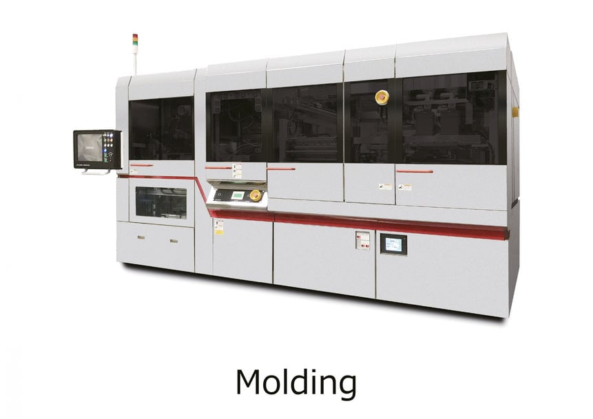
High performance molding system.
Back-End Processes and Solutions
The portfolio covers die and flip chip bonding, with equipment that offers accuracy down to ±5μm in X- Y and ±0.5° in θ (3-sigma) and incorporates advanced features including a twin-head design with unique servo-drive technology that saves space and boosts productivity.
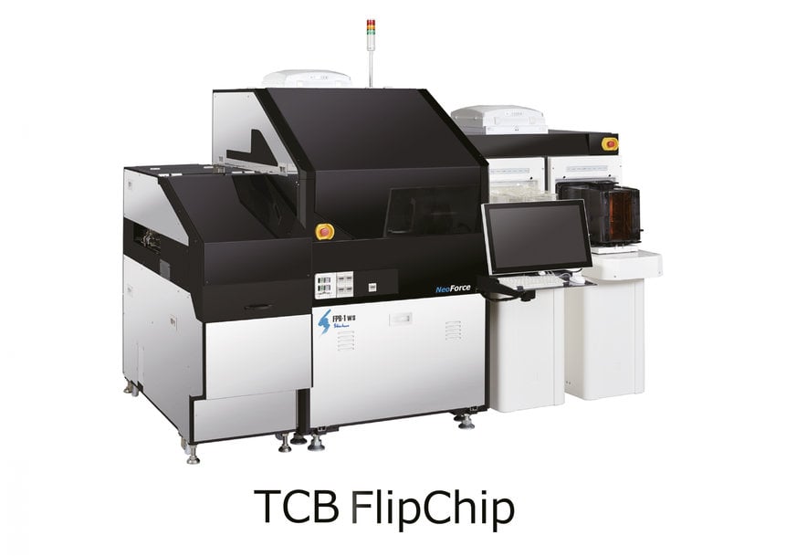
Die bonders offer flexibility with support for face-down and face-up bonding, thin-wafer handling, and support for 2.5D and 3D stack. Processes supported include thermo-compression bonding with non- conductive paste (TCB-NCP), non-conductive film (TCB-NCF), Thermo-Compression-Capillary Underfill (TC-CUF), and standard and fan-out wafer-level packaging (FO-WLP). The Shinkawa FPB- 1w NeoForce Package Bonder (figure 1) handles NCP/NCF/TC-CUF, C2 and C4, and FO-WLP, with automatic product-type changeover.
There are also wire bonders that offer positional accuracy within 2μm and high speed up t0 45ms/2mm, and high-accuracy bump bonding with technologies to ensure stable quality and handling for various standard wafer sizes. The UTC5000NeoCu wire bonder can handle wires from 18-70μm diameter and offers user convenience through features such as inert-gas control by recipe selection and templates that simplify looping optimisation.
By developing processes such as ultrasonic bonding at low temperature, which is fast and eliminates thermal stress on components and materials, the portfolio also includes equipment for packaging specific product types such as crystal components like temperature-controlled oscillators (TCXOs) and surface-acoustic wave (SAW) filters as well as LEDs and CMOS ICs.
Precision dispensing equipment in the portfolio can handle various processes including dispensing LED fluorescent materials, underfill materials, and adhesives for assembling crystal devices for frequency control applications. Solutions for high-accuracy and high-speed crystal-blank mounting, low-particle adhesive curing, package inspection and testing, simultaneous multi-crystal frequency adjustment, and TCXO temperature test provide a complete set of capabilities for packaging and testing crystal devices.

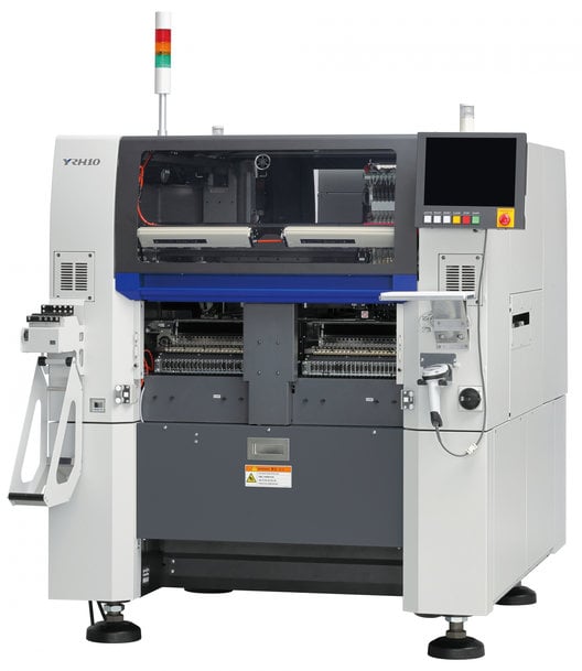
The YRH10 hybrid flip-chip bonder and surface-mounter launched in 2021.
Multi-Die Devices and Modules
Yamaha has already established a portfolio of flip-chip mounters including the YSB55w flip chip bonder that has ±5μm accuracy and capabilities including 8-die simultaneous pickup and simultaneous transfer that enable 13,000 UPH placement speed.
In July 2021, Yamaha introduced a major update to its hybrid range that combines multi-chip back-end die bonding and surface-mount component assembly. The new machine, YRH10 (figure 3), raises production capability by 50% over the preceding generation and increases placement accuracy to ±15μm, thanks to new features including a multi-nozzle head, accelerated wafer swaps, and improved thermal compensation.
When combined with the UTC5000NeoCu wire bonder from the Shinkawa portfolio, the YRH10 has demonstrated a complete assembly process for MEMS microphone production. The process comprises placement and bonding of MEMS chip and ASIC to the substrate, interconnection of the two chips by wire bonding, adhering the package metal cap.
The YRH10 has also combined with Yamaha’s YSM10 entry-level high-speed modular surface-mount placement machine for power module assembly. The two machines take care of placing IGBT dies on direct bonded copper (DBC) substrate, mounting the substrate onto the module’s thermal baseplate, placing solder preforms for die and substrate attachment, and placing associated sensors and drivers.
Conclusion
Increasing the share of semiconductor manufacturing fulfilled from within Europe can potentially deliver economic, logistical and environmental benefits, by shortening supply chains and localising access to cutting-edge ICs. Moves have been announced at government level, seeking participation from industrial partners. In addition to investment in design and fabrication facilities, chip and module packaging capabilities are also needed. Yamaha’s investment in technologies for back-end automation, creating Yamaha Robotic Holdings, makes advanced solutions available to Europe’s manufacturers.
www.fa.yamaha-motor-im.de

