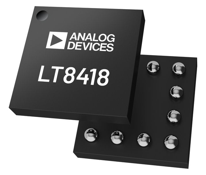
Analog Devices’ GaN Driver Enables Robust and Reliable Control of GaN FETs
Analog Devices, Inc. (ADI) now offers a 100V half-bridge GaN driver that simplifies the implementation of GaN FETs, proving robust gate control, high frequency switching, and increased system efficiency.

Integrating top and bottom driver stages, driver logic control, and protections, the new LT8418 can be configured into synchronous half-bridge, full-bridge topologies, or buck, boost, and buck-boost topologies. The device provides strong current sourcing/sinking capability with 0.6 pull-up and 0.2Ω pull-down resistance for driving a variety of GaN FETs. It also integrates a smart integrated bootstrap switch to generate a balanced bootstrap voltage from VCC with a minimum dropout voltage.
The LT8418 delivers split gate drivers to adjust the turn-on and turn-off slew rates of GaN FETs to suppress ringing and optimize EMI performance. All driver inputs and outputs have default low-state to prevent GaN FETs from false turn-on. The pulsed width modulation inputs of the LT8418, INT and INB, are independent and TTL logic compatible for precise control. The LT8418 performs with a fast propagation delay of 10ns and maintains a delay matching of 1.5ns between the top and bottom channels, making it suitable for high-frequency DC-DC converters, motor drivers, and class-D audio amplifiers. In addition, the LT8418 employs the WLCSP package to minimize parasitic inductance, enabling its wide use in high-performance and high-power density applications.
Product Specifications
- Split 0.6Ω pullup and 0.2Ω pulldown gate drivers for adjustable turn on/off behavior
- 4A peak source, 8A peak sink current capability
- Lower propagation delay: 10ns typical
- Propagation delay matching: 1.5ns typical
- High dv/dt immune up to 50V/ns
- Under-Voltage (VCC & BST) and Over-Voltage (VCC) lockout protections
- Smart integrated bootstrap switch will regulate the HS gate drive voltage to operate within the SOA of the GaN FETs

