
electronics-journal.com
24
'24
Written on Modified on
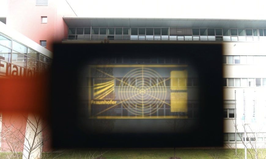
Transparent emissive microdisplays for ultra-light and compact augmented reality systems
As part of the HOT project (High-performance transparent and flexible microelectronics for photonic and optical applications), scientists from the Fraunhofer Institute for Photonic Microsystems IPMS have developed a semi-transparent microdisplay.
More and more augmented-reality (AR) glasses and see-through systems with different application areas are entering the market. To increase the acceptance of these devices and improve wearing comfort, it is important that they are lightweight and easy to use. For mobile consumer electronics devices, the key acceptance criteria are form factor or compactness (volume, weight), battery life, connectivity, app ecosystem, and cost.
OLED microdisplays are ideal as image generators for virtual-reality (VR), augmented-reality (AR), and mixed-reality (MR) applications, due to their high resolution and technological level/maturity. However, these microdisplays are typically not transparent due to their silicon-based technology. Therefore, a complex optical system is required for use in see-through data glasses and similar devices, which allows the combination of real and virtual images (optical combiner). This has significant implications on the weight, size, and optical efficiency of the entire glasses. Current optical see-through near-to-eye displays (NTE) in augmented-reality devices attempt to solve the form factor problem through various technical approaches, such as coupling images from non-transparent image sources into waveguide or fold element optics.
The scientists at the Fraunhofer Institute for Photonic Microsystems IPMS have years of experience in developing innovative designs for novel microdisplays and possess a globally unique expertise in this field. Thanks to their newly developed semi-transparent OLED-on-silicon microdisplay technology, completely new possibilities for optical design of slim, near-eye optics are being opened up.
Philipp Wartenberg, Group manager IC and System Design at Fraunhofer IPMS, explains: "Modern and advanced silicon CMOS processes are increasingly being applied to silicon-on-insulator (SOI) wafers. This wafer technology can be used for implementation of very thin circuitry layers. With the help of a specific IC design and an appropriate process flow which enables transfer on a glass wafer semi-transparent microdisplays are possible."
Depending on the design approach, microoptics can already be directly integrated on the chip. The transparent microdisplay itself becomes an optical combiner element, significantly reducing the size of the optical system and improving optical efficiency significantly. Further internal technology studies indicate that transparencies of over 50% are achievable.
The scientists are pleased with the successful first technology demonstrator of the transparent microdisplay. They continue to work on increasing transparency and are ready for customer- and application-specific developments to bring this novel technology to market readiness.
www.ipms.fraunhofer.com
