
electronics-journal.com
30
'25
Written on Modified on
Keysight EDA and Intel Foundry Collaborate on EMIB-T Silicon Bridge Technology
Supports latest interconnect standards, including Universal Chiplet Interconnect Express™ 2.0 and Open Compute Project Bunch of Wires, for improved design flexibility.
www.keysight.com
Keysight Technologies announced a collaboration with Intel Foundry to support Embedded Multi-die Interconnect Bridge-T (EMIB-T) technology, a cutting-edge innovation aimed at improving high-performance packaging solutions for artificial intelligence (AI) and data center markets in addition to the support of Intel 18A process node.
As the demands of AI and data center workloads continue to grow in complexity, ensuring reliable communication between chiplets and 3DICs is becoming increasingly critical. High-speed data transfer and efficient power delivery are essential to meet the performance demands of next-generation semiconductor applications. The semiconductor industry addresses these challenges through emerging open standards, such as Universal Chiplet Interconnect Express™ (UCIe™) and Bunch of Wires (BoW). These standards define interconnect protocols for chiplets and 3DICs within advanced 2.5D/3D or laminate/organic packages, enabling consistent, high-quality integration across different design platforms.
By adopting these standards and verifying chiplets for compliance and link margin, Keysight EDA and Intel Foundry contribute to a growing chiplet interoperability ecosystem. The collaboration aims to reduce development costs, mitigate risk, and accelerate innovation in semiconductor design.
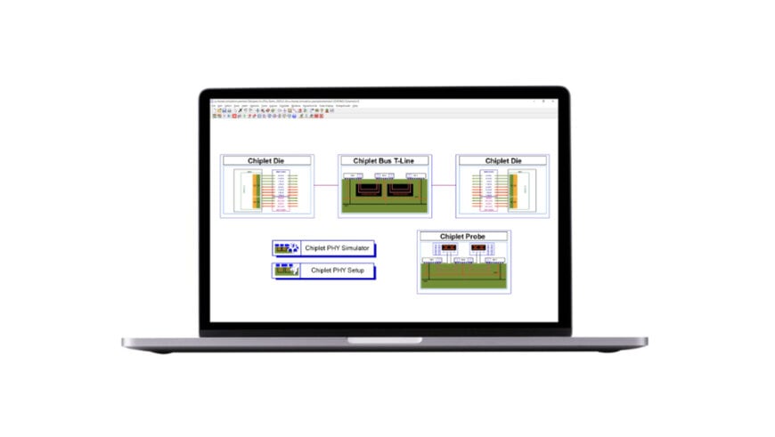
Keysight EDA’s Chiplet PHY Designer, the latest solution for high-speed digital chiplet design tailored to AI and data center applications, now offers advanced simulation capabilities for the UCIe™ 2.0 standard and introduces support for the Open Computer Project BoW standard. As an advanced, system-level chiplet design and die-to-die (D2D) design solution, Chiplet PHY Designer enables pre-silicon level validation, streamlining the path to tapeout.
www.keysight.com
