
electronics-journal.com
27
'25
Written on Modified on
Basler Revolutionizes TGV Inspection for Semiconductors
Basler's patented vision solution delivers fast, clear, full inspection of Through Glass Vias, addressing challenges in semiconductor panel-level packaging.
www.baslerweb.com
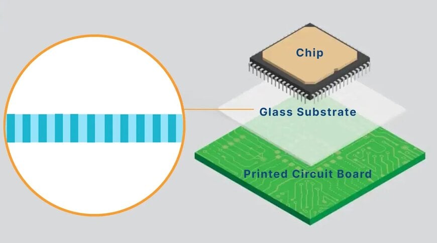
As the semiconductor industry accelerates toward Panel-Level Packaging (PLP) and glass-core substrates to meet the demands of AI, HPC, and advanced chiplet architectures, traditional inspection methods are falling short. The shift to large-format glass panels introduces new challenges—and new opportunities. At Basler, we've developed a patented inspection solution tailored for high-density TGV inspection on glass substrates. Our vision solution delivers one-pass, full inspection with industry-leading clarity and speed.
Critical inspection points in the TGV manufacturing process
Glass substrate manufacturing involves multiple precision processes—from via laser drilling and wet etching to metallization and copper filling—each requiring rigorous quality control. As high-density interconnects become standard in advanced packaging, it is critical to ensure that all vias are present and free from defects. Missing or malformed vias can lead to serious downstream failures and costly yield losses. Inspection must verify proper via formation, metallization, and structural integrity across the entire panel. Thorough glass substrate inspection is the essential first step toward reliable, high-performance packaging.
One-scan TGV inspection: maximize throughput with no blind spots
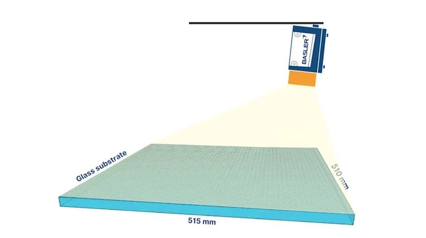
Current AOI systems struggle with full-area inspection of large glass substrates (e.g., 510 mm x 500 mm) used in Through Glass Via (TGV) manufacturing, often compromising between inspection area, resolution, and throughput. Critical micro-defects—such as cracks, bubbles, sidewall roughness, and misaligned double-conical vias—frequently go undetected, particularly due to the transparent nature of the material and the complexity of 3D via structure.
One-scan precision. Zero blind spots.
Our patented one-scan TGV inspection solution overcomes these challenges by combining vision system optical design, high resolution imaging and advanced image processing algorithms, delivering:
- Full-panel inspection in a single scan with no blind spots
- Robust detection of complex defects including conicity misalignment, edge chipping, and depth inconsistencies
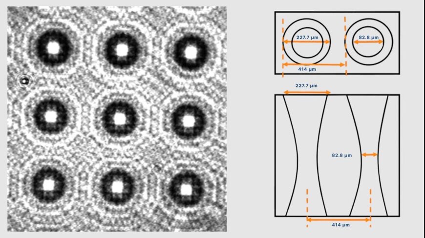
- Micron-level analysis of taper angle, sidewall integrity, via depth, pitch, and diameter
This integrated vision solution provides images with excellent contrast for accurate, high-throughput TGV inspections, significantly improving process control and yield in advanced substrate manufacturing.
www.baslerweb.com
www.baslerweb.com
