
electronics-journal.com
22
'26
Written on Modified on
Vertical Transistor Integration Through Stacked Nanosheet Architecture
Samsung Electronics advances semiconductor scaling by vertically integrating transistors to maximize spatial efficiency for next-generation logic devices.
semiconductor.samsung.com
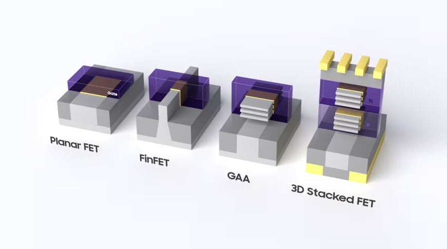
[Figure 1] Evolution of transistor architectures: Planar FET → FinFET → GAA → 3D Stacked FET
Samsung Electronics has introduced a 42-nanometer gate-pitch three-dimensional stacked field-effect transistor, utilizing triple-stacked nanosheet channels to advance semiconductor manufacturing. This architectural evolution vertically integrates n-type and p-type transistors to increase component density for advanced logic applications within the global semiconductor ecosystem.
Evolution of Transistor Architecture and Vertical Integration
The transition from planar and FinFET architectures to Gate-All-Around configurations improved electrostatic control over the channel. As logic circuits require continuous physical scaling, expanding horizontally by placing n-type and p-type transistors side by side presents distinct spatial limitations. Vertically stacking these components reduces the functional footprint of the cell. During the 2026 VLSI Symposium held from June 14 to 18, the Semiconductor Research Center detailed this methodology. The submitted research received an evaluation score of 8.29 out of 10, indicating a measurable structural impact on semiconductor device fabrication protocols.
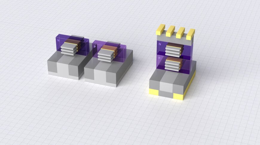
[Figure 2] Comparison between planar n-type/p-type transistor placement and vertically stacked transistor placement
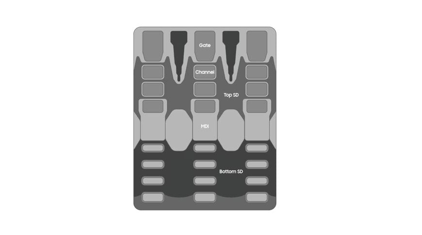
Enhancing Current Conduction with Triple-Stacked Channels
Maintaining sufficient drive current within a reduced functional area requires multiple conduction paths. The structural implementation involves triple-stacked nanosheet channels for both the upper and lower transistors. This configuration preserves the effective channel width necessary for robust electrical performance while operating within a confined vertical footprint. By optimizing the epitaxial growth process, the fabricated silicon-based crystal layers maintain uniform thickness and structural integrity. Consistent crystalline quality across multiple layers ensures uniform current transport and minimizes electrical variability across the semiconductor manufacturing ecosystem.
[Figure 3] Cross-sectional view of the 3D Stacked FET structure
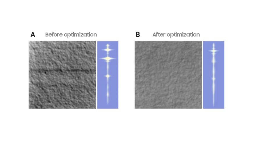
[Figure 4] Comparison of crystal layer uniformity
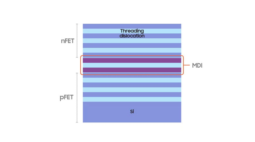
Mitigating Electrical Coupling via Middle Dielectric Isolation
Positioning n-type and p-type transistors in strict vertical proximity necessitates precise electrical isolation to prevent signal interference. This requirement is addressed through the integration of a Middle Dielectric Isolation layer. The isolation barrier physically separates the upper and lower devices while providing a calibrated structural reference for the formation of distinct gate stacks. Fabricating this layer requires exact thickness control; a disproportionately thin layer permits electrical coupling, whereas an excessively thick layer impedes the precise formation of the necessary gate materials.
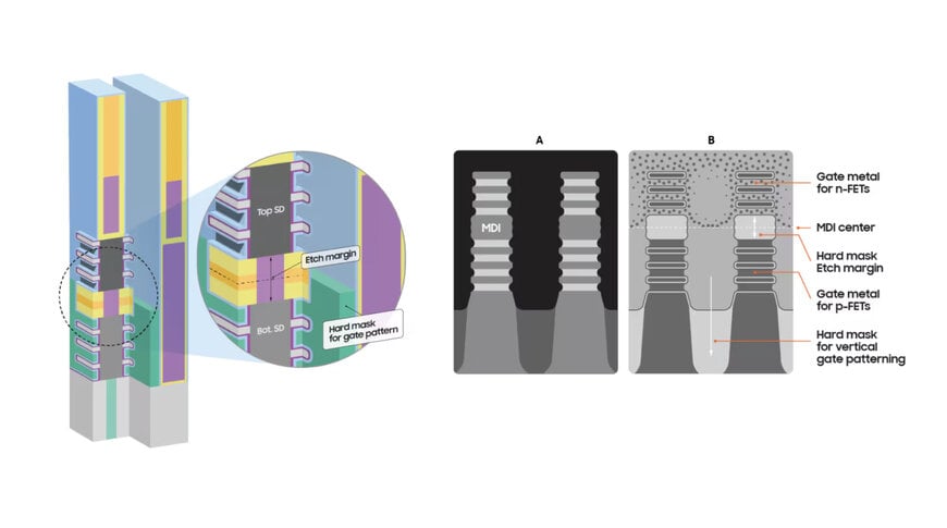
[Figure 5] Cross-sectional view of a 3D Stacked FET structure
[Figure 6] 3D Stacked FET Wafer Cross Section (TEM)
Demonstrating Practical Application at a 42-Nanometer Gate Pitch
The structural feasibility of this three-dimensional field-effect transistor was validated through the fabrication of a device featuring a 42-nanometer gate pitch. This metric, defining the distance between adjacent gates, dictates the maximum achievable component density on a wafer. Testing validated the current-control characteristics of the vertically stacked n-type and p-type transistors, confirming minimal leakage during off-states and adequate conduction during active states. Device uniformity was also verified across multiple wafer samples, a mandatory requirement for scaling architecture into mass production.
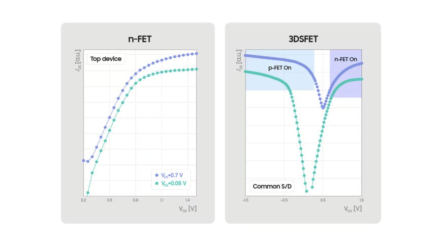
[Figure 7] Current-control characteristics of the 3D Stacked FET
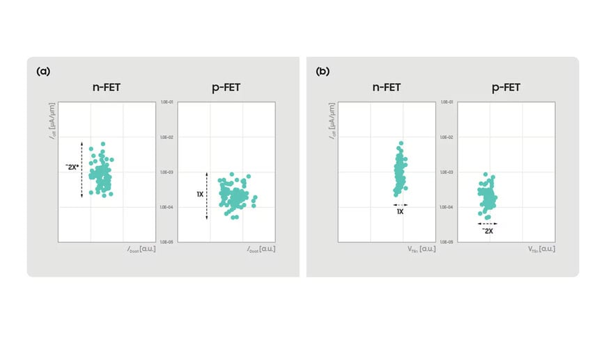
[Figure 8] Electrical performance variation and process impact in 3D Stacked FETs
a) Impact of source/drain epitaxy on Ioff–IDsat characteristics
b) Impact of bottom source/drain etch profile on Ioff–VTlin characteristics
Additional Context:
This section details technical specifications and competitive benchmarking not included in the original product announcement
The three-dimensional stacked field-effect transistor, fundamentally recognized in the semiconductor industry as a Complementary Field-Effect Transistor, operates within a competitive sector focused on sub-50-nanometer logic scaling. Intel and TSMC maintain parallel research trajectories aimed at standard cell area reduction. Analytical data indicates that while conventional Gate-All-Around architectures limit spatial efficiency, monolithic Complementary Field-Effect Transistor designs target cell area reductions of up to 50 percent. Competitive benchmarks generally position these developmental structures at a 45 to 50-nanometer gate pitch, establishing the 42-nanometer implementation by Samsung Electronics as a highly dense physical integration. The vertical separation methodology utilized functions comparably to standard dielectric integration techniques pursued by competing foundries to isolate active monolithic channels without signal degradation.
Edited by Natania Lyngdoh, Induportals editor, assisted by AI.
www.semiconductor.samsung.com
Samsung Electronics has introduced a 42-nanometer gate-pitch three-dimensional stacked field-effect transistor, utilizing triple-stacked nanosheet channels to advance semiconductor manufacturing. This architectural evolution vertically integrates n-type and p-type transistors to increase component density for advanced logic applications within the global semiconductor ecosystem.
Evolution of Transistor Architecture and Vertical Integration
The transition from planar and FinFET architectures to Gate-All-Around configurations improved electrostatic control over the channel. As logic circuits require continuous physical scaling, expanding horizontally by placing n-type and p-type transistors side by side presents distinct spatial limitations. Vertically stacking these components reduces the functional footprint of the cell. During the 2026 VLSI Symposium held from June 14 to 18, the Semiconductor Research Center detailed this methodology. The submitted research received an evaluation score of 8.29 out of 10, indicating a measurable structural impact on semiconductor device fabrication protocols.
[Figure 2] Comparison between planar n-type/p-type transistor placement and vertically stacked transistor placement
Enhancing Current Conduction with Triple-Stacked Channels
Maintaining sufficient drive current within a reduced functional area requires multiple conduction paths. The structural implementation involves triple-stacked nanosheet channels for both the upper and lower transistors. This configuration preserves the effective channel width necessary for robust electrical performance while operating within a confined vertical footprint. By optimizing the epitaxial growth process, the fabricated silicon-based crystal layers maintain uniform thickness and structural integrity. Consistent crystalline quality across multiple layers ensures uniform current transport and minimizes electrical variability across the semiconductor manufacturing ecosystem.
[Figure 3] Cross-sectional view of the 3D Stacked FET structure
[Figure 4] Comparison of crystal layer uniformity
Mitigating Electrical Coupling via Middle Dielectric Isolation
Positioning n-type and p-type transistors in strict vertical proximity necessitates precise electrical isolation to prevent signal interference. This requirement is addressed through the integration of a Middle Dielectric Isolation layer. The isolation barrier physically separates the upper and lower devices while providing a calibrated structural reference for the formation of distinct gate stacks. Fabricating this layer requires exact thickness control; a disproportionately thin layer permits electrical coupling, whereas an excessively thick layer impedes the precise formation of the necessary gate materials.
[Figure 5] Cross-sectional view of a 3D Stacked FET structure
[Figure 6] 3D Stacked FET Wafer Cross Section (TEM)
Demonstrating Practical Application at a 42-Nanometer Gate Pitch
The structural feasibility of this three-dimensional field-effect transistor was validated through the fabrication of a device featuring a 42-nanometer gate pitch. This metric, defining the distance between adjacent gates, dictates the maximum achievable component density on a wafer. Testing validated the current-control characteristics of the vertically stacked n-type and p-type transistors, confirming minimal leakage during off-states and adequate conduction during active states. Device uniformity was also verified across multiple wafer samples, a mandatory requirement for scaling architecture into mass production.
[Figure 7] Current-control characteristics of the 3D Stacked FET
[Figure 8] Electrical performance variation and process impact in 3D Stacked FETs
a) Impact of source/drain epitaxy on Ioff–IDsat characteristics
b) Impact of bottom source/drain etch profile on Ioff–VTlin characteristics
Additional Context:
This section details technical specifications and competitive benchmarking not included in the original product announcement
The three-dimensional stacked field-effect transistor, fundamentally recognized in the semiconductor industry as a Complementary Field-Effect Transistor, operates within a competitive sector focused on sub-50-nanometer logic scaling. Intel and TSMC maintain parallel research trajectories aimed at standard cell area reduction. Analytical data indicates that while conventional Gate-All-Around architectures limit spatial efficiency, monolithic Complementary Field-Effect Transistor designs target cell area reductions of up to 50 percent. Competitive benchmarks generally position these developmental structures at a 45 to 50-nanometer gate pitch, establishing the 42-nanometer implementation by Samsung Electronics as a highly dense physical integration. The vertical separation methodology utilized functions comparably to standard dielectric integration techniques pursued by competing foundries to isolate active monolithic channels without signal degradation.
Edited by Natania Lyngdoh, Induportals editor, assisted by AI.
www.semiconductor.samsung.com
