
electronics-journal.com
28
'26
Written on Modified on
Multilayer Ceramic Substrate for AI Semiconductor Packaging
Kyocera Corporation introduces a rigid ceramic core substrate to address warpage and wiring density limits in advanced AI and ASIC semiconductor packaging.
global.kyocera.com
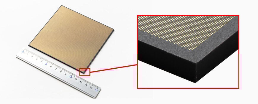
Advanced semiconductor packaging for AI data centers is facing increasing constraints in substrate stability and wiring density. Kyocera Corporation has developed a multilayer ceramic core substrate designed to improve mechanical rigidity and enable finer interconnect structures in high-performance xPU and ASIC packages.
Addressing Packaging Constraints in AI Data Infrastructure
The rapid expansion of AI workloads, including large language models, is driving demand for high-performance processors such as CPUs and GPUs collectively referred to as xPUs. These devices are typically integrated into complex packages used in data center infrastructure, where substrate size and interconnect density continue to increase.
Conventional organic core substrates present limitations in this context. As substrate dimensions grow, susceptibility to warpage becomes a critical issue, affecting assembly yield and long-term reliability. In parallel, finer wiring requirements challenge the limits of mechanical drilling processes used in organic materials.
Kyocera’s multilayer ceramic core substrate is designed to mitigate these issues through higher structural rigidity and improved microfabrication capabilities. The technology is intended for use in 2.5D packaging architectures, where multiple integrated circuits are mounted on a shared interposer to enhance processing performance and bandwidth in the automotive data ecosystem and large-scale AI computing environments.
Ceramic Material Design and Warpage Reduction
The substrate is based on Kyocera’s Fine Ceramic materials and incorporates a multilayer structure that increases resistance to deformation. Higher rigidity reduces bending during thermal cycling and assembly processes, which are typical causes of warpage in large-format semiconductor packages.
According to company simulations conducted in February 2026, the ceramic-based design enables thinner substrates while maintaining structural integrity. This reduction in warpage contributes to improved alignment accuracy during component mounting and supports higher device performance by maintaining consistent electrical interconnect geometry.
High-Density Wiring Through Advanced Via Formation
A key feature of the multilayer ceramic substrate is the formation of vias during the material’s pliable state, prior to sintering. This approach differs from conventional organic substrates, where vias are mechanically drilled after material curing.
By forming vias at this earlier stage, the process enables smaller via diameters of approximately 75 µm and tighter via pitches of around 200 µm. These parameters support higher interconnect density and improved signal routing efficiency, which are critical for high-bandwidth applications such as AI accelerators and switch ASICs.
The resulting three-dimensional wiring structure allows more compact circuit layouts, addressing miniaturization requirements in next-generation semiconductor devices used in the digital supply chain and hyperscale computing systems.
Simulation-Driven Design Integration
Kyocera integrates simulation capabilities into the substrate design phase, including thermal, electrical, and warpage modeling. These simulations are aligned with specific device requirements and mounting processes, enabling optimization before physical prototyping.
This approach supports reduced development cycles and improves the likelihood of meeting performance targets in final semiconductor assemblies. It is particularly relevant for custom designs in high-performance computing, where thermal management and signal integrity are tightly coupled with substrate characteristics.
Industry Context and Application Scope
The multilayer ceramic core substrate will be presented at the Electronic Components and Technology Conference (ECTC 2026), scheduled for May 26–29, 2026, in Orlando, Florida. The event focuses on advancements in semiconductor packaging technologies.
The technology is positioned for applications in AI data centers, high-performance computing, and advanced networking systems. It is particularly suited to 2.5D integration schemes, where substrate performance directly impacts overall system efficiency.
By addressing the mechanical and scaling limitations of organic substrates, ceramic-based alternatives represent a potential pathway for supporting continued increases in semiconductor performance and integration density.
Edited by an industrial journalist Sucithra Mani with AI assistance.
www.kyocera.com
