
electronics-journal.com
20
'26
Written on Modified on
High-Density Quasi-Monolithic Chiplet Integration at Wafer Level
Fraunhofer IPMS has developed a quasi-monolithic integration method utilizing structured silicon pockets to embed chiplets for advanced heterogeneous semiconductor manufacturing.
www.fraunhofer.de
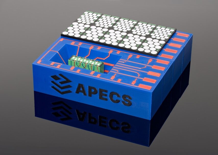
3D printing of a demonstrator for quasi-monolithic integration with a chiplet in the pocket.
The demand for increased computing power and system compactness in microelectronics requires alternative approaches to semiconductor manufacturing. Addressing the physical limitations of traditional chip packaging, researchers are focusing on quasi-monolithic integration (QMI). This approach enables disparate chip components, including control electronics, sensors, and microelectromechanical systems (MEMS), to be combined directly at the wafer level. The technology targets highly integrated system-on-chip (SoC) architectures for artificial intelligence processing and high-bandwidth smart transceivers, bridging the gap between compact single-chip designs and modular multi-chip systems.
Technical Mechanism and Wafer-Level Embedding
Within the European APECS pilot line, which concentrates on advanced packaging and heterogeneous integration for electronic components, the Fraunhofer Institute for Photonic Microsystems (Fraunhofer IPMS) has validated the primary physical integration phase of the QMI process. The methodology relies on utilizing silicon wafers equipped with structured recesses. Dummy chiplets are inserted into these specific pocket wafers, after which the surface is planarized using a passivation layer.
"The basis of QMI is silicon wafers with structured recesses, or pockets. For the first time, dummy chiplets have been inserted into these pocket wafers and the surface has been levelled with a passivation layer in preparation for subsequent back-end-of-line wiring," stated Dr. Lukas Lorenz, group leader at Fraunhofer IPMS. "This creates a nearly monolithic system architecture that combines the highest integration density with modular scalability."
Operational Parameters and System Performance
QMI technology provides a distinct structural arrangement compared to conventional packaging processes. Chiplets are positioned on an active or passive wafer substrate sharing a common interconnect stack. Because the interconnects are established during the front-end-of-line process, the resulting connection densities are higher than those achieved through traditional back-end packaging methods. The reduction of signal paths decreases latency and mitigates power losses, thereby altering processing speeds at the system level. Furthermore, minimizing mechanical interfaces increases the overall structural robustness and operational lifecycle of the semiconductor systems. The integration method reduces spatial requirements, allowing for highly compact modular chiplet assemblies.
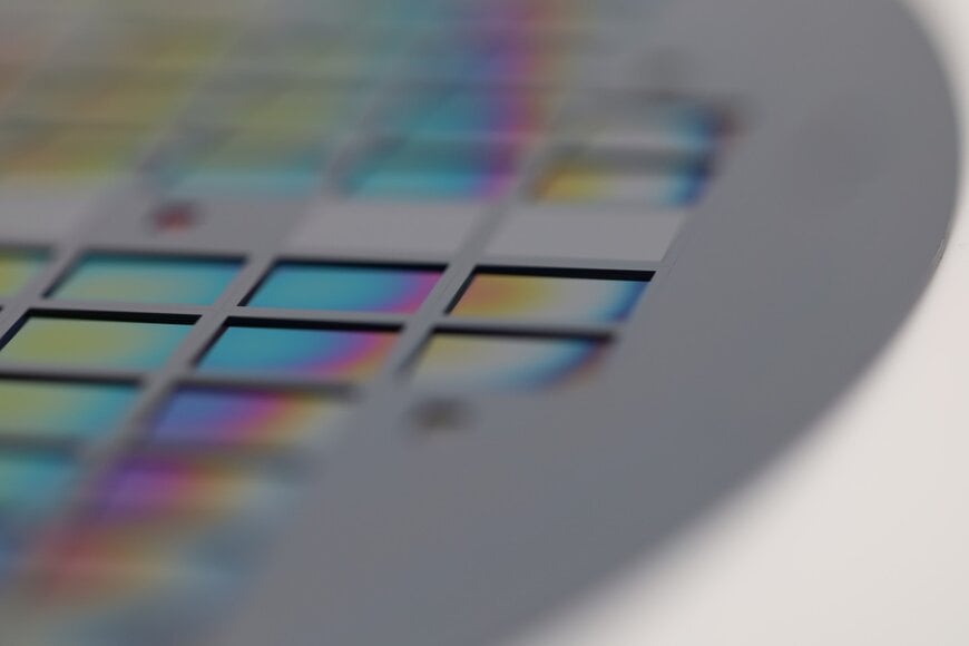
Wafer with placed chiplets.
Industrial Transfer and Scalability
The current demonstrator utilizes dummy structures to validate the mechanical and chemical integration steps required for embedding. The established process chain is designed for transferability to functional customer applications requiring high-density heterogeneous system architectures. The methodologies validated under the APECS framework provide a standardized foundation for migrating QMI technology into production-oriented semiconductor manufacturing environments.
Additional Context: This section details technical specifications and competitive benchmarking not included in the original product announcement
Existing high-density semiconductor packaging solutions, such as 2.5D silicon interposers and 3D through-silicon via (TSV) stacking, offer high interconnect densities but entail complex micro-bump arrays to route signals between disparate dies. Commercial benchmarks, such as TSMC's CoWoS (Chip-on-Wafer-on-Substrate) or Intel's Foveros, utilize these micro-bumps and interposers to achieve heterogeneous integration. In contrast, the QMI approach embeds chiplets directly into wafer pockets and planarizes the surface to utilize standard front-end-of-line interconnects for routing. This method theoretically eliminates the need for micro-bumps between the chiplet and the substrate, which can lower interconnect pitch limits and reduce the vertical profile of the final package compared to standard 2.5D or 3D integration techniques.
Edited by an industrial journalist, Lekshman Ramdas, with AI assistance.
www.fraunhofer.com
The demand for increased computing power and system compactness in microelectronics requires alternative approaches to semiconductor manufacturing. Addressing the physical limitations of traditional chip packaging, researchers are focusing on quasi-monolithic integration (QMI). This approach enables disparate chip components, including control electronics, sensors, and microelectromechanical systems (MEMS), to be combined directly at the wafer level. The technology targets highly integrated system-on-chip (SoC) architectures for artificial intelligence processing and high-bandwidth smart transceivers, bridging the gap between compact single-chip designs and modular multi-chip systems.
Technical Mechanism and Wafer-Level Embedding
Within the European APECS pilot line, which concentrates on advanced packaging and heterogeneous integration for electronic components, the Fraunhofer Institute for Photonic Microsystems (Fraunhofer IPMS) has validated the primary physical integration phase of the QMI process. The methodology relies on utilizing silicon wafers equipped with structured recesses. Dummy chiplets are inserted into these specific pocket wafers, after which the surface is planarized using a passivation layer.
"The basis of QMI is silicon wafers with structured recesses, or pockets. For the first time, dummy chiplets have been inserted into these pocket wafers and the surface has been levelled with a passivation layer in preparation for subsequent back-end-of-line wiring," stated Dr. Lukas Lorenz, group leader at Fraunhofer IPMS. "This creates a nearly monolithic system architecture that combines the highest integration density with modular scalability."
Operational Parameters and System Performance
QMI technology provides a distinct structural arrangement compared to conventional packaging processes. Chiplets are positioned on an active or passive wafer substrate sharing a common interconnect stack. Because the interconnects are established during the front-end-of-line process, the resulting connection densities are higher than those achieved through traditional back-end packaging methods. The reduction of signal paths decreases latency and mitigates power losses, thereby altering processing speeds at the system level. Furthermore, minimizing mechanical interfaces increases the overall structural robustness and operational lifecycle of the semiconductor systems. The integration method reduces spatial requirements, allowing for highly compact modular chiplet assemblies.
Wafer with placed chiplets.
Industrial Transfer and Scalability
The current demonstrator utilizes dummy structures to validate the mechanical and chemical integration steps required for embedding. The established process chain is designed for transferability to functional customer applications requiring high-density heterogeneous system architectures. The methodologies validated under the APECS framework provide a standardized foundation for migrating QMI technology into production-oriented semiconductor manufacturing environments.
Additional Context: This section details technical specifications and competitive benchmarking not included in the original product announcement
Existing high-density semiconductor packaging solutions, such as 2.5D silicon interposers and 3D through-silicon via (TSV) stacking, offer high interconnect densities but entail complex micro-bump arrays to route signals between disparate dies. Commercial benchmarks, such as TSMC's CoWoS (Chip-on-Wafer-on-Substrate) or Intel's Foveros, utilize these micro-bumps and interposers to achieve heterogeneous integration. In contrast, the QMI approach embeds chiplets directly into wafer pockets and planarizes the surface to utilize standard front-end-of-line interconnects for routing. This method theoretically eliminates the need for micro-bumps between the chiplet and the substrate, which can lower interconnect pitch limits and reduce the vertical profile of the final package compared to standard 2.5D or 3D integration techniques.
Edited by an industrial journalist, Lekshman Ramdas, with AI assistance.
www.fraunhofer.com
