
electronics-journal.com
05
'26
Written on Modified on
Ultratrace Analysis Improves Wafer Surface Quality Control
Fraunhofer IPMS introduced advanced wafer surface contamination analysis services to help semiconductor manufacturers detect ultratrace elements and improve semiconductor production quality.
www.fraunhofer.de
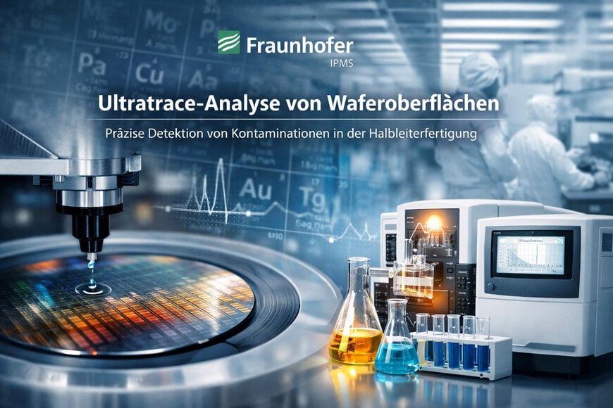
Manufacturers of microchips rely on semiconductor wafers with extremely clean and chemically stable surfaces. Even trace levels of metallic or chemical contamination can affect the functionality, yield, and reliability of semiconductor devices. As semiconductor structures continue to shrink, quality control requirements for wafer surfaces have become increasingly stringent.
To support semiconductor manufacturers in addressing these challenges, the Fraunhofer Institute for Photonic Microsystems IPMS expanded its analytical services to include ultratrace elemental analysis for wafer surfaces. The new capability allows semiconductor companies to identify contamination at extremely low concentrations and better understand surface-related production issues.
Analytical Solution for Detecting Ultratrace Contamination
The institute implemented an analytical method combining vapor phase decomposition with inductively coupled plasma mass spectrometry (VPD-ICP-MS). This approach enables highly sensitive detection and quantification of soluble contaminants present on wafer surfaces.
During the analysis process, wafers with diameters of 200 mm or 300 mm are exposed to hydrofluoric acid vapor to dissolve surface residues. A droplet is then applied to the wafer and moved across the surface while the wafer rotates. The droplet collects dissolved contaminants before being diluted to a defined volume for measurement.
The collected sample is subsequently analyzed using ICP-MS, providing precise quantitative information about trace elements on the wafer surface.
Surface and Bevel Scanning for Detailed Characterization
The analytical method supports both surface scans and bevel scans, enabling detailed mapping of contamination across the wafer. Using a hydrofluoric acid scan solution, up to 39 elements can be analyzed during the characterization process.
For applications requiring detection of noble metals, aqua regia scanning solutions can be applied, enabling targeted analysis of five noble metal elements.
This capability allows semiconductor manufacturers to investigate contamination sources, evaluate process cleanliness, and monitor wafer quality during production.
Laboratory Infrastructure Supporting Semiconductor Quality Control
To support the new analytical services, the Fraunhofer IPMS laboratory is equipped with specialized measurement and preparation systems. These include the WSPS2 Wafer Surface Preparation System from PVA Tepla and the iCap RQ mass spectrometer from Thermo Scientific.
The combination of wafer preparation technology and high-sensitivity mass spectrometry enables accurate characterization of wafer surfaces and supports quality assurance processes in semiconductor fabrication.
Supporting Semiconductor Production Reliability
By expanding its analytical capabilities, Fraunhofer IPMS provides semiconductor manufacturers with additional tools to detect contamination sources and maintain high wafer quality standards.
The ultratrace element analysis service contributes to improved process monitoring and supports manufacturers in maintaining reliable semiconductor production in increasingly complex fabrication environments.
www.ipms.fraunhofer.com
