
electronics-journal.com
03
'26
Written on Modified on
Ionized Sputtering for Glass Substrate Packaging
TRUMPF introduces an industrial plasma generation process designed to coat high-density through-glass vias, facilitating rapid data transmission in artificial intelligence processors.
www.trumpf.com
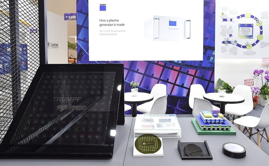
TRUMPF is releasing its High-Power Impulse Magnetron Sputtering (HiPIMS) product line, a specialized system for the reliable metallization of complex glass substrates in the semiconductor sector. This technology enables manufacturers to coat the microscopic structures required for next-generation artificial intelligence chips and high-performance computing applications.
Integration Within the Semiconductor Packaging Ecosystem
The hardware requirements for artificial intelligence processors dictate integrating more computational functions into smaller footprints while increasing internal data transmission speeds. To meet these specifications, semiconductor manufacturers are transitioning to glass substrates instead of traditional organic materials. This advanced packaging architecture requires drilling millions of microscopic holes, known as through-glass vias (TGVs), into the substrate and subsequently coating them with conductive materials to route electrical signals.
A primary failure mechanism in this process is the uneven application of conductive material. The required holes feature high aspect ratios, meaning they are deeply penetrating and extremely narrow. A minimal number of incorrectly coated through-vias is sufficient to render an entire glass panel electrically unusable, severely impacting mass production viability.
Directed Ionization and Magnetic Plasma Control
The HiPIMS process addresses the spatial challenges of deep-trench metallization through high-performance plasma generation. The industrial generators produce a highly ionized plasma containing a significantly higher proportion of electrically charged particles compared to conventional sputtering methods. By applying synchronized electric and magnetic fields, the system precisely directs these ionized particles into the narrow vias.
This controlled directionality results in a substantially higher density of deposited molecules and a uniform coating along the vertical walls of the trenches. Piotr Lach, Head of Next Technology Demands at TRUMPF Elektronik, notes that high-density through-glass vias are integral to future chip generations, making the reliable coating of millions of fine structures a mandatory requirement for maintaining manufacturing yield.
Scaling High-Yield Industrial Production
Establishing a stable process with consistent results is the baseline for transitioning new packaging concepts into commercial series production. The highly ionized deposition process mitigates typical structural defects, thereby increasing the overall yield of functional components. In industrial manufacturing environments, this coating phase operates in tandem with other critical hardware systems. Facilities typically utilize ultrashort-pulse lasers to physically drill the initial through-glass vias before employing specialized plasma power supplies for the subsequent coating and etching cycles.
Additional Context
This section details technical specifications and competitive benchmarking not included in the original news release.
In the domain of advanced semiconductor packaging, the metallization of high-aspect-ratio through-glass vias (TGVs) generally relies on competing physical vapor deposition (PVD) and chemical deposition techniques. Standard Direct Current (DC) magnetron sputtering provides high throughput but struggles to achieve adequate step coverage in deep, narrow vias, frequently resulting in void formation and incomplete sidewall coverage. Conversely, Atomic Layer Deposition (ALD) offers near-perfect conformality for complex topographies but operates at exceedingly low deposition rates, limiting its cost-effectiveness for mass metallization.
HiPIMS functions as a structural midpoint, producing ionization fractions that frequently exceed 70% for sputtered metals. This high degree of ionization allows for the perpendicular acceleration of ions toward the substrate, achieving dense, void-free coverage at the bottom and sidewalls of deep TGVs while maintaining continuous deposition rates that fulfill the strict throughput requirements of commercial semiconductor fabrication facilities.
Edited by Aishwarya Mambet, Induportals Editor, with AI assistance.
www.trumpf.com
