
electronics-journal.com
24
'26
Written on Modified on
Siemens & TSMC Automate Advanced Semiconductor Node Design
New agentic workflows accelerate physical verification, thermal analysis, and packaging integration across sub-2nm processes and silicon photonics architectures.
www.siemens.com
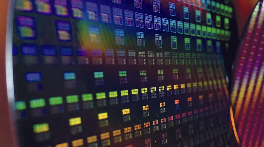
Siemens Digital Industries Software and Taiwan Semiconductor Manufacturing Company (TSMC) are collaborating to integrate artificial intelligence into electronic design automation (EDA) environments for advanced integrated circuit (IC) manufacturing. The joint technical initiative targets digital and custom IC design, multi-die 3D packaging, and silicon photonics across sub-2nm process nodes.
Operational Challenges in Sub-2nm and Multi-Die Architecture
Shrinking process geometries down to the A14 and A16 nodes introduce severe physical verification complexities, including increased design rule constraints, electromigration risks, and thermal dissipation challenges. Concurrently, multi-die architectures such as wafer-level 3D chip stacking and chip-on-wafer configurations require co-design across heterogeneous dies, photonic engines, and substrates. Addressing these multidimensional physical constraints demands tighter synchronization between foundry design rules and automated layout, verification, and simulation tools.
Autonomous Design Rule Checking and Implementation Workflows
Siemens has implemented the Fuse EDA AI system to execute autonomous, multi-step verification routines. Under this framework, an AI agent coordinates Calibre, Aprisa, and Solido software engines to automatically identify, analyze, and correct design rule check (DRC) violations. Aprisa provides automated place-and-route convergence alongside pre-simulation-driven die-to-die autorouting to maintain signal integrity parameters. The framework uses contextual design rule data to execute automated fixes directly within digital and custom flows, reducing iterative manual intervention during tapeout preparation.
3D Packaging and Silicon Photonics Integration
The engineering teams have qualified Calibre 3DStack Advanced software with multi-machine execution to handle inter-chiplet antenna verification for TSMC-SoIC and CoWoS-L architectures. Calibre 3DThermal software has achieved static and transient thermal analysis certification for TSMC A16 and system-on-wafer reference flows, with ongoing reference flow development for the TSMC Compact Universal Photonic Engine (COUPE).
For silicon photonics, the integrated flow incorporates Innovator3D IC Integrator, Solido Simulation Suite, and L-Edit software to verify optical transceiver interfaces. Solido Simulation Suite also supports pulse-amplitude modulation 4-level (PAM4) electrical measurements for COUPE optical links.
Advanced Node Certification
Physical verification tools, including Calibre nmDRC, Calibre nmLVS, Calibre xACT, and Calibre PERC, are certified for the TSMC A14 node. For electrical reliability, the mPower platform is certified for transistor-level power grid electromigration and voltage drop (IR-drop) analysis on TSMC N2P and N3C nodes, with validation extending to A14. Solido Simulation Suite is certified for SPICE simulation accuracy on N3C, A16, and A14 technologies, providing variation-aware analysis, IC aging modeling, and self-heating verification for custom and analog circuits.
Edited by Natania Lyngdoh, Induportals editor, assisted by AI.
www.siemens.com
