
electronics-journal.com
15
'26
Written on Modified on
Keysight at ECOC 2026
From September 21–23, in Málaga, Spain, Keysight Technologies demonstrates testing systems to validate optical interconnects and artificial intelligence networks for data center deployments.
www.keysight.com
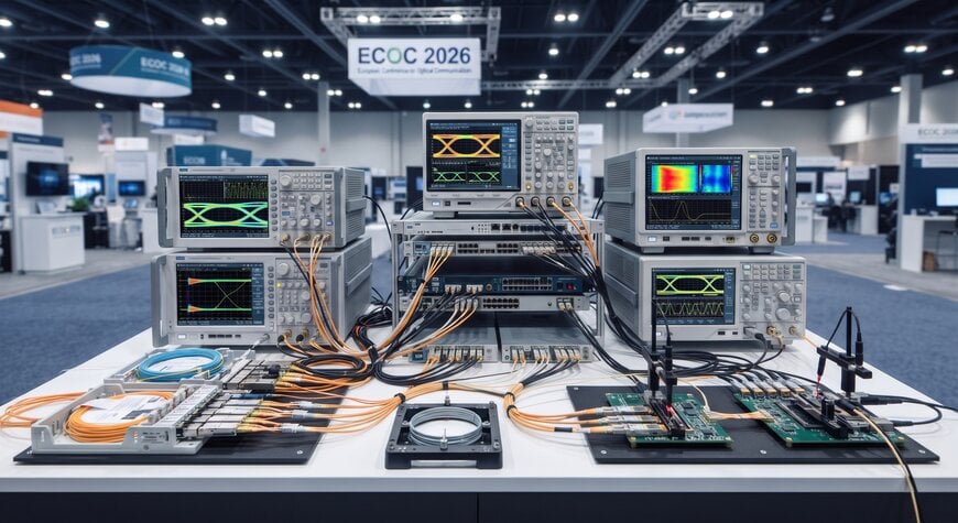
Keysight Technologies announced measurement workflows designed to characterize optical links and validate computing fabrics used in data centers. The demonstrations target transmission bottlenecks and interconnect scaling across high-bandwidth computational infrastructure.
Operational Challenges in Optical Networks
Data center operators face signal integrity degradation and latency challenges as transmission rates expand to 1.6T and 3.2T architectures. Integrating photonic integrated circuits (PIC) requires continuous data correlation between component-level simulation and volume assembly lines to maintain production yield. Concurrently, clusters deployed for AI model training and distributed inference demand deterministic interconnect performance under sustained load. Addressing these constraints requires specialized test platforms capable of measuring ultra-wide bandwidths while emulating multi-node network traffic.
Technical Solution and Measurement Architecture
Keysight Technologies configured a test suite targeting both physical-layer validation and transport-layer verification:
- Photonic Design and Characterization: The platform integrates optical circuit simulation directly with automated PIC probing. High-frequency electrical and electro-optical characterization reaches bandwidths up to 220 GHz, aligning simulation models with wafer-level and package-level physical behavior.
- Multi-Terabit Link Validation: The architecture provides transmitter and receiver validation for 1.6T transceivers, alongside research instrumentation configured for 3.2T optical interfaces. This instrumentation evaluates modulation formats, jitter parameters, and bit error ratios to mitigate physical-layer interface margin risks.
- AI Fabric and Workload Emulation: Hardware emulators generate real-world traffic profiles to stress-test high-speed fabric fabrics, benchmarking data transport throughput, queue management, and latency during parallelized compute operations.
- Automated Test Execution: Algorithms manage measurement sequencing, anomaly detection, and data aggregation, reducing cycle times for optical characterization.
Implementation and Industrial Deployment
The test frameworks were presented at the European Conference on Optical Communication (ECOC), held September 21–23, 2026, at FYCMA in Málaga, Spain. Demonstrations at booth #1154 demonstrated integration points where test equipment interfaces with industrial assembly equipment and optical manufacturing execution systems.
Industrial Applications and Operational Impact
The system supports component manufacturers, transceiver developers, and hyperscale cloud providers. Concrete applications include:
The test frameworks were presented at the European Conference on Optical Communication (ECOC), held September 21–23, 2026, at FYCMA in Málaga, Spain. Demonstrations at booth #1154 demonstrated integration points where test equipment interfaces with industrial assembly equipment and optical manufacturing execution systems.
Industrial Applications and Operational Impact
The system supports component manufacturers, transceiver developers, and hyperscale cloud providers. Concrete applications include:
- Photonic Foundry Verification: Automating parameter extraction during wafer sorting to identify defective dies prior to packaging.
- Production Line Scaling: Implementing parallelized optical power and spectrum measurements to decrease per-unit test duration during 1.6T transceiver manufacturing.
- Data Center Fabric Qualification: Validating switch-to-optical interfaces under emulated compute bursts to ensure link stability and avoid transport-layer packet loss.
Correlating automated optical measurements with physical-layer simulation provides engineering teams with measurable performance data across design iterations, supporting consistent production ramp phases for multi-terabit infrastructure.
Edited by Evgeny Churilov, Induportals Media - Adapted by AI.
www.keysight.com
Edited by Evgeny Churilov, Induportals Media - Adapted by AI.
www.keysight.com
