
electronics-journal.com
29
'26
Written on Modified on
Murata Unveils the World Smallest RF Microwave Switch Connector
Engineered to reduce board mounting area by forty percent, these compact components deliver superior high frequency performance for dense modern mobile and communication devices.
www.murata.com
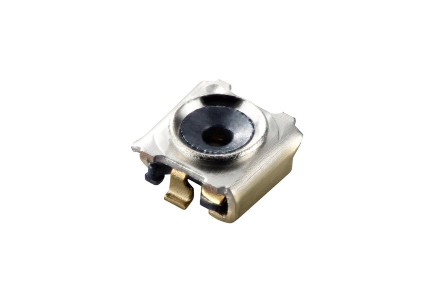
As wireless devices become increasingly sophisticated, the growing component count has led to severe PCB space constraints. Consequently, minimizing keep-out areas to prevent interference with test fixtures has emerged as a critical challenge in circuit design. To meet these demands for high-density mounting, Murata Manufacturing Co., Ltd. began mass production in August 2026 of the SWL series of RF coaxial connectors with switch—models "MM8330-2600RJ5" and "MM8330-2600RK20"—achieving an ultra-compact 1.0 mm square profile.
Reduction of PCB Footprint via Ultra-Compact RF Switch Mechanism
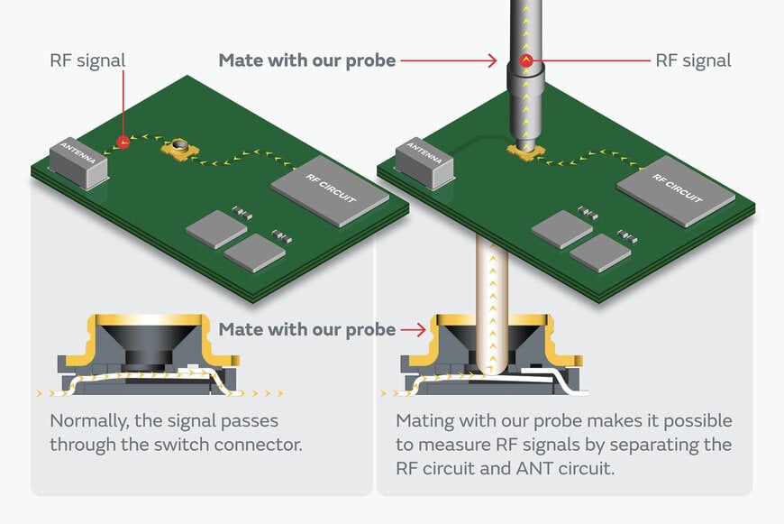
In high-density wireless communication modules for smartphones, wearable devices, and various IoT equipment, RF circuit verification is essential for maintaining production yield during mass manufacturing. An RF coaxial connector with switch serves a mechanical switching function: during standard operation, it maintains an electrical connection along the signal path to the internal antenna; when mated with a dedicated probe during the testing phase, it automatically disconnects the internal circuit and routes the RF signal directly to the measurement instrument.
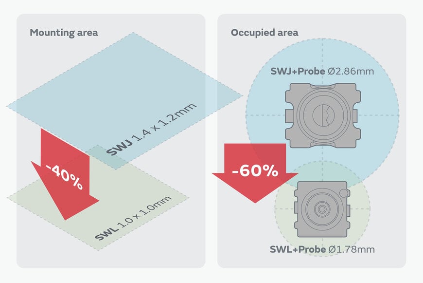
The newly developed SWL series adopts an ultra-compact, low-profile design measuring 1.0 mm × 1.0 mm × 0.55 mm (L × W × H). Compared to Murata’s conventional SWJ series (1.4 mm × 1.2 mm × 0.65 mm), it reduces the standalone mounting footprint by approximately 40%. Leveraging a proprietary internal structure that fuses high-frequency design expertise with precision mechanical engineering, the connector suppresses RF transmission loss—a common pitfall of miniaturization—while maintaining mechanical durability against repeated probe insertion and extraction.
Reduction of Keep-Out Areas in Testing Processes and Enhanced Productivity
When selecting coaxial connectors with switch, PCB layout constraints depend not only on the physical mounting dimensions of the connector body, but also on reserving a keep-out zone to prevent the measurement probe from colliding with adjacent components during engagement. By co-designing dedicated automated probes and dedicated manual probes (scheduled for mass production in December 2026) tailored to this compact connector, Murata minimized this interference zone.
When combined with the dedicated probe, the total occupied area is reduced by approximately 60% compared to conventional solutions. This allows adjacent passive components and shield cans to be placed in closer proximity to the connector, substantially increasing PCB layout flexibility while mitigating transmission losses associated with long trace routing. Streamlining signal verification on mass-production lines facilitates early defect detection, reduces material scrap, and prevents design rework, contributing to overall productivity gains across the manufacturing line.
Additional Information
This section details technical specifications and competitive benchmarks not covered in the original product announcement.
In the market for switched coaxial connectors used in wireless communication equipment, accommodating higher frequency bands such as 5G millimeter-wave and Wi-Fi 7 has made low insertion loss and favorable voltage standing wave ratio (VSWR) across wide bandwidths the standard evaluation benchmarks. Typical RF switch connectors support frequencies ranging from DC up to approximately 6 GHz, with select variants reaching 11 GHz or higher, utilizing internal transmission lines matched to a 50 Ω characteristic impedance.
Key market competitors include the Hirose Electric (HIROSE) MS-156 series, I-PEX MHF-series switches, and direct-probe compact test terminals. Conventional standard inspection switch connectors (typically measuring 1.8 mm × 1.8 mm to 1.4 mm × 1.2 mm) required an effective PCB footprint of roughly 1.7 mm² to 3.2 mm². Furthermore, the added keep-out zone dictated by probe outer diameters (typically 2.0 mm to 3.0 mm) posed an inherent structural challenge by significantly enlarging the prohibited routing zone on the board.
In contrast, Murata’s SWL series shrinks the form factor down to 1.0 mm × 1.0 mm (1.0 mm² footprint) and optimizes both the probe outer diameter and the lead-in guide mechanism to substantially compress the total footprint. While competitors like Hirose also offer compact, low-profile solutions, commercializing an integrated-switch connector within a 1.0 mm square profile and a 0.55 mm height sets a new design benchmark for high-density SMT assembly in wearable devices and ultra-compact communication modules.
Edited by Evgeny Churilov, Induportals Media - Adapted by AI.
www.murata.com
