
electronics-journal.com
03
'26
Written on Modified on
Qualcomm Validates High Bandwidth Compute Silicon To Advance AI Inference
New silicon testing validates innovative memory architecture designed to increase bandwidth, reduce data movement, and deliver superior energy efficiency for data center artificial intelligence workloads.
www.qualcomm.com
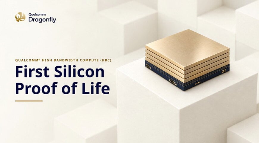
Qualcomm Technologies and advanced semiconductor manufacturing partners are collaborating to implement near-memory computing architectures for data center infrastructure. The technical initiative integrates Qualcomm High Bandwidth Compute (HBC) silicon into modular compute systems to reduce data transfer latency and energy dissipation in large-scale artificial intelligence inference deployments.
Scaling Challenges in Digital Infrastructure
Large language model inference requires sequential weight transfers for each generated token. Conventional server architectures encounter a memory wall where interconnect bandwidth limits processing throughput, inflating electrical power consumption and total cost of ownership. Addressing this physical scaling barrier requires integrating logic and dynamic random-access memory (DRAM) within unified three-dimensional packages to shorten physical interconnect distances.
Engineering Collaboration and Silicon Architecture
Qualcomm Technologies leads the architectural design, defect mapping, and logic development, while specialized foundry and outsourced semiconductor assembly and test partners manage physical integration. The collaborative process qualifies multi-generation wafer-to-wafer bonding to stack DRAM tiers directly onto underlying logic base dies.
Near-memory computing places computational nodes directly adjacent to memory arrays, reducing signal transit distance and parasitic capacitance. The joint engineering framework incorporates defect remapping, electrical redundancy, and thermal mitigation layers to manage operational stress and interconnect yields across bonded structural interfaces.
Hardware Validation and Test Integration
Engineers verified first-generation silicon in laboratory environments using standard automated test equipment across production-representative dimensions. The testing protocol drove synthetic workloads through complete memory read-write channels, processing randomized weights and activations.
Validation confirmed mechanical integrity across the bonding planes and verified operational signaling along data pathways. Active product tape-outs have advanced to logic base dies bonded with multi-tier DRAM stacks to confirm structural repeatability and thermal dissipation under standard operational tolerances.
Infrastructure Integration and Product Roadmap
The joint technology targets hyperscale cloud data centers and high-density industrial automation facilities requiring energy-efficient inference execution. Integrating high-bandwidth compute architectures enables continuous token generation with reduced energy draw per computational cycle.
The validated silicon provides the foundational layer for the Qualcomm Dragonfly AI250 accelerator, scheduled for sampling in early 2027. The accelerator will integrate into the disaggregated Qualcomm Dragonfly Rack system, providing enterprise cloud facilities with standardized, power-optimized inference hardware.
Edited by Evgeny Churilov, Induportals Media - Adapted by AI.
www.qualcomm.com
