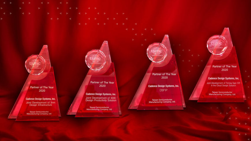
Cadence Wins Four 2020 TSMC OIP Partner of the Year Awards
Cadence achieves recognition for joint development of N3 design infrastructure, 3D-IC design productivity solution, timing signoff in the cloud design solution and DSP IP.

Cadence Design Systems, Inc. (Nasdaq: CDNS) today announced that it has received four OIP Partner of the Year awards from TSMC for IP and EDA solutions. Cadence achieved recognition for the joint development of the N3 design infrastructure, 3D-IC design productivity solution, timing signoff in the cloud design solution and DSP IP.
These awards were given to Cadence based on the following work that has been delivered:
- N3 design infrastructure: Cadence participated in an in-depth collaboration with TSMC on the design infrastructure development of this advanced process technology and has been working with customers using the Cadence® Virtuoso® Custom IC design platform and a full suite of digital design, implementation and signoff tools anchored by the Innovus Implementation System and Genus Synthesis Solution on N3 production designs.
- 3D-IC design productivity solution: Cadence collaborated with TSMC on significant productivity enhancements to design solutions for the latest TSMC 3DFabric packaging technologies, delivering certified and enhanced reference flows for InFO and CoWoS® that include a full suite of Cadence multi-chip and chiplet advanced package planning, layout, verification and electrical analysis, including the Clarity 3D Solver for 3D electromagnetic modeling for CoWoS designs.
- Timing signoff in the cloud design solution: Cadence further expanded its cloud collaboration with TSMC by demonstrating methodologies to accelerate timing signoff with the Cadence Tempus Timing Signoff Solution via the Cadence CloudBurst Platform, showing scalability on 150 machines for the fastest turnaround time and methods that reduce timing-signoff machine costs by 2X. Also, Cadence successfully delivered secure cloud-based environments for universities creating advanced-node designs and teaming with TSMC’s Cloud Alliance partners to provide a design environment for TSMC’s first-ever IC Layout Contest. Each of these areas leveraged the CloudBurst Platform to meet TSMC’s Virtual Design Environment (VDE) requirements.
- DSP IP: Cadence worked with TSMC’s Soft IP9000 team to certify Cadence Tensilica® DSP IP in the TSMC integration flow.
“We’ve consistently worked with Cadence to enable our mutual customers to achieve the best possible design results,” said Suk Lee, senior director of the Design Infrastructure Management Division at TSMC. “We look forward to seeing our customers leverage the design solutions using our latest advanced technologies to deliver new silicon innovations with fast time-to-market in their respective markets.”
“Through our ongoing collaboration with TSMC, we’re enabling mutual customers to deliver designs with confidence and meet design goals using our newest technologies,” said Dr. Chin-Chi Teng, senior vice president and general manager of the Digital & Signoff Group at Cadence. “These prestigious awards from TSMC further indicate Cadence’s commitment to delivering upon its Intelligent System Design strategy, which enables customers to achieve SoC design excellence across a variety of key market areas ranging from hyperscale computing to consumer segments.”
www.cadence.com

