Hidden heroes realizing a low-carbon economy – The future of power semiconductors
The Japanese government’s fall 2020 decision to realize carbon neutrality by 2050 quickly attracted a lot attention, and a lot of public support.

- Key devices for power management and control, and a carbon-free future
- Harvesting Toshiba’s strengths in manufacturing and group collaboration
- Toward next-generation devices and production on larger wafers
A Cabinet Office poll, “Public Opinion Survey on Climate Change,” found that 91.9% of respondents would “like to work on the realization of a carbon-free society.” And this is far from unique to Japan. In the United States, President Biden has made countering climate change one of his most important policies, and announced the goals of decarbonization of the power sector by 2035, and net zero greenhouse gas emissions by 2050. The UK amended its Climate Change Act in 2019, to stipulate that the country will be carbon neutral by 2050.
The whole world is moving towards decarbonization and carbon neutrality. Decarbonization is fast emerging as a global trend, and semiconductors are going to be the key to its realization—more specifically, power semiconductors. To find out more we spoke to Takeshi Kamebuchi of Toshiba Electronic Devices & Storage Corporation, and shone a spotlight on the hidden heroes in the shadows—power semiconductors, and their leading role in helping us to achieve a low-carbon future. We asked Kamebuchi to explain the background and Toshiba’s strategy.
Power semiconductors: key devices for a low-carbon economy
Power semiconductors manage the supply and control of power—electric power, that is. Simply explained they play the role of an on-off switch, but by switching on and off at very high speed they can convert direct and alternating current, raise and lower voltages, and convert power frequencies.
Kamebuchi, who heads Toshiba’s semiconductor business, comes up with an apt analogy: “If we compare semiconductors to parts of the body, processors and memories can be seen as the brain, but power semiconductors play the role of the heart and muscles.”

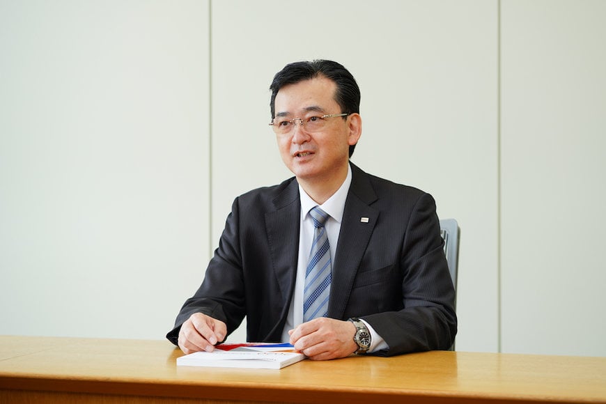
Takeshi Kamebuchi, Vice President, Semiconductor Division Toshiba Electronic Devices & Storage Corporation
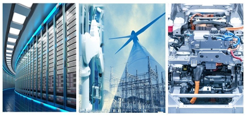
They are also as essential as the heart and muscles, and handle power control in all kinds of electrical equipment, ranging from TVs, washing machines and other home appliances to key infrastructure equipment, including rolling stock and power transmission and distribution equipment. Improving the performance of power semiconductors reduces power loss, and directly contributes to reducing the power consumption of equipment.
When we look to the realization of a carbon-free economy, the lion’s share of attention goes to decarbonization of power generation, particularly the use of renewable energy. But making much more efficient use of electricity is just as important. Power semiconductors are small devices that make a big contribution to decarbonization through the “smart use” of power, and that explains why they are seen as key devices for a carbon-free, low-energy future.

Power semiconductors are installed in all electrical equipment
Strengths realized by manufacturing power and group collaboration
Among the ways that these hidden heroes of a carbon-free tomorrow differ from other semiconductors is that Toshiba and other Japanese manufacturers maintain a strong presence in the market. This is all due to “manufacturing power.” The structure of power semiconductors must allow large vertical current flows from the drain to the source of the chip. Performance varies depending on how that structure is created, and getting it right requires both optimizing technologies and manufacturing know-how. The general perception of the semiconductor industry is that whoever makes the largest capital investment will win, but alongside that factor, manufacturing power is also a source of competitiveness in power semiconductor business.
Kamebuchi explains just what this means in practice. “Toshiba’s power semiconductors have a long track record of application in areas where quality is a must, such as automobiles. The manufacturing know-how and technology that we have cultivated in our long history is not something that can be imitated overnight. I remember back to when I was working on the factory floor, and I felt there was a really strong on-site motivation to make good things and to make improvements. I really believe that this kind of intangible technological capability also adds value to our products.”
Alongside manufacturing power, Toshiba can also point to the strength of group collaboration. Toshiba Group is large and diverse, with divisions that work on products like inverters for rolling stock or infrastructure for power transmission and distribution. As Kamebuchi see it, undertaking product development while taking on feedback from these users helps to launch timely products that really meet market needs. He also welcomes the ability to collaborate on next-generation technology development with Toshiba Group’s research labs. “With the collective strength of Toshiba Group we are going to expand the power semiconductor business and contribute to the realization of a carbon-free future,” he says enthusiastically.
The responsibilities of semiconductor manufacturers
While the performance of power semiconductors is contributing to the realization of a carbon-free economy, there is more to the equation than that. One factor that must be considered is the manufacturing process. The manufacture of semiconductors, of whatever type, generally requires a lot of electricity, water, chemicals and gases. However much power semiconductors might improve the energy-saving performance of equipment, if their manufacture consumes a lot of energy, then their net impact on energy consumption and the Earth will be diminished.
Kamebuchi is crystal clear on this: “Reducing the environmental burdens of the manufacturing process is the responsibility and highest priority of companies that manufacture semiconductors. When we provide the market with energy-efficient products, we must also be aware of impacts on the environment, and make continuing efforts to control them. Only when these two wheels are in alignment are we truly contributing to the realization of a low-carbon future.”
The numerous initiatives Toshiba is promoting in the manufacturing process include cutting electricity for air-conditioning by using waste heat from the production buildings—something not done until now—and reducing the volume of purified water for cleaning when manufacturing equipment is on standby. The efforts made by Japan Semiconductor Corporation, a Toshiba Group company, were recently recognized with the 2020 Japanese Minister of the Environment Award, presented for contributing to the realization of a recycling-oriented society.
Ensuring the future of the business
In March 2021, Toshiba made an important decision toward ensuring the future of its power semiconductor business: to invest in larger diameter wafers production facility.
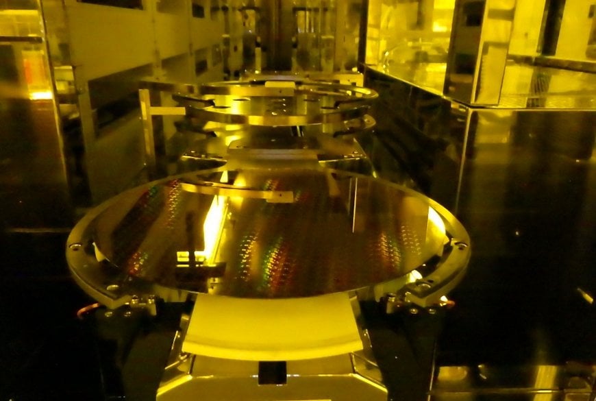
Semiconductors are manufactured on discs of silicon, known as wafers. Larger wafers yield more chips, and production is more efficient. However, power semiconductors have long been characterized as high-mix low-volume products, and manufacturing has been done on 200mm wafers, with production on 300mm wafers reserved for low-mix, mass-produced semiconductors such as memories and CPUs. This is starting to change, and recent years has seen an accelerating trend, mainly among major overseas manufacturers, toward producing power semiconductors on 300mm wafers.
There are good reasons to make the transition. The electrification of automobiles, automation of industrial equipment, widespread use of inverter technology in home appliances, and the expanded use of renewable energy, are all contributing to increased demand for power semiconductors. Sufficient sales can now be expected to justify production on 300mm wafers.
In addition to boosting production efficiency, 300mm wafer lines can also contribute to improved semiconductor performance, and wafer vendors leave more room for capacity expansion of 300mm wafer—all considerations that make manufacturing on them attractive. However, these benefits all come with a cost, and an enormous investment is required to be able to work with the larger wafers. We asked Kamebuchi about the background to the decision.
“Yes, of course, the initial investment carries a large cost. However, with moves toward a low-carbon future, the market is expanding significantly, and competition is intensifying. I see the next few years as a major inflection point for the power semiconductor business, and if we are to survive in the business, now is the best time to make this move. Being the first Japanese semiconductor manufacturer with a 300mm wafer production line will provide Toshiba with a big weapon in respect of supply and quality. Naturally, alongside production efficiency, we will also continue to refine our high-precision process technologies.”

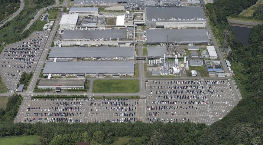
An aerial view of the 300mm wafer facility at Kaga Toshiba Electronics Corporation, Ishikawa prefecture, Japan
Looking to the future: next generation devices
” It soon becomes clear that Kamebuchi is looking even further ahead than his words first suggest. Alongside production on larger diameter there is another force in play: new materials that are expected to have a major impact.
Most semiconductors are made of silicon, but in some applications, particularly those requiring high voltage and high speed switching, silicon is pushing the limits of its physical characteristics. Continued progress and better next-generation performance will require compound semiconductor materials, and two that are attracting strong attention are silicon carbide (SiC) and gallium nitride (GaN). They are expected to deliver dramatic improvements over silicon devices.”
To be more specific, these new materials support improved device power efficiency, and with that it becomes possible to significantly reduce system power consumption, and also to advance system miniaturization. Adoption of SiC-based semiconductors has already started with inverters for railways, and Toshiba semiconductors are in use in a lot of new rolling stock. Even so, there are still many problems to solve before compound semiconductors find widespread application, especially in respect of manufacturing cost and reliability. Today, we are at the point where development is advancing, and Toshiba and other companies are preparing for a full-scale market launch.
“In terms of research and development, the next few years will be a major turning point,” Kamebuchi says with animation. “We will also focus on developing next-generation power semiconductors, so that we can be ready for provide high-performance products as soon as possible.”
Balancing prosperity and a sustainable society
Although only small chips, hidden away in all kinds of electronic equipment and devices, the immense contributions power semiconductors make to power control and energy gives them great potential to contribute to a low-carbon tomorrow. As he readies himself for major changes in the business environment, including production on larger diameter wafers and development of new materials, Kamebuchi speaks strongly with an eye to the future.
“As long as people continue to use electricity, power semiconductors will remain essential, and improving their performance is a must if we are to achieve both an affluent future and a sustainable society. Power semiconductors are where Toshiba’s semiconductor business is most closely focused. We will do all we can to accelerate the expansion of production capacity and to develop new technologies, so that we can contribute to the realization of a carbon-free society.”
Keep an eye on what happens to power semiconductors from now on—hidden heroes in the realization of a carbon-free future.
www.toshiba.com

