electronics-journal.com
15
'21
Written on Modified on
Renesas Develops Write Technologies for Embedded STT-MRAM Significantly Reducing MCUs Power Consumption in IoT Applications
Announced at IEDM 2021: Confirmed Reduced Power Consumption and Increased Speed in Write Operations on 16 nm FinFET Logic Process Embedded STT-MRAM Test Chip.

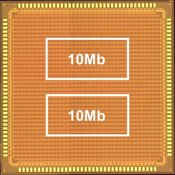
Renesas Electronics Corporation (TSE:6723), a premier supplier of advanced semiconductor solutions, today announced the development of two technologies that reduce the energy and voltage application time for the write operation of spin-transfer torque magnetic random-access memory (STT-MRAM, hereinafter MRAM). On a 20-megabit (Mbit) test chip with embedded MRAM memory cell array in a 16 nm FinFET logic process, a 72 percent reduction in write energy and a 50 percent reduction in the voltage application time were confirmed.
The new technologies are: 1) A self-termination write scheme with slope pulse application, in which the write pulse is automatically and adaptively terminated due to write characteristics of each memory cell; 2) A write sequence to optimize the number of bits, to which write voltage is applied simultaneously. Combined, these technologies make it possible to reduce the power consumption and increase the speed of write operations.
Renesas presented these achievements on December 13 at the 2021 IEEE International Electron Devices Meeting (IEDM), held between December 11 and 15 in San Francisco.
With the accelerated spread of IoT technology in recent years, there has been strong demand for reduced power consumption in microcontroller units (MCUs) used in endpoint devices. MRAM requires less energy for write operations than flash memory, and is thus particularly well suited for applications with frequent data updates. However, as demand for data processing capability surges for MCUs, the need to ameliorate the trade off between performance and power consumption increases. Therefore, further power consumption reduction remains a pressing issue.
The new MRAM write technologies addressing this need are described below.
1. Self-Termination Write Scheme Utilizing Slope Pulses
Binary data is stored in MRAM by using the high-resistance state (HRS) and low-resistance state (LRS) of magnetic tunnel junction (MTJ) devices to represent values of 1 and 0, respectively. Previously, a self-termination write scheme has been proposed to reduce the write energy and voltage application time, by detecting the write completion through monitoring the memory cell current during fixed write voltage application, and automatically halting the application of the write voltage. However, issues related to factors, such as variation in memory cell characteristics and the detection accuracy of the comparator circuit to detect write completion, have prevented the successful implementation of stable and consistent detection of write completion.
To address these issues, instead of applying a fixed voltage during write operation where the MTJ changes from HRS to LRS in a conventional self-termination write, a slope voltage that rises gradually over time has been adopted. This makes it possible to detect write completion stably and consistently. Even when the memory cell current does not reach the detection level of the detector circuit immediately after state transition due to variation in memory cell characteristics and other factors, the subsequent gradual rise in the write voltage increases the memory cell current. This eventually exceeds the detection level, enabling the completion of the write to be detected and application of the write voltage to be halted.
During write operation where the state transition is in the opposite direction, from LRS to HRS, the memory cell current changes from a large to a small current, so write completion detection using a slope voltage pulse is not possible. Therefore, a current source circuit is used to increase the write current in a sloping manner, and write completion is detected by monitoring the write voltage with a voltage detector circuit to determine if it exceeds a pre-set judgement voltage.
2. Simultaneous Write Bit Number Optimization Technique
Previously, the MRAM write voltage was determined based on the worst bit write characteristics in the memory cell characteristics variation. This meant that a high write voltage was necessary, and a charge pump circuit was used to generate it. In order to reduce the area and power consumption of the charge pump circuit, the write unit of the MRAM macro was divided into four or more multiple groups, for example, and each write pulse was applied sequentially. However, this increased the write voltage application time by the number of divisions.
To resolve this issue, Renesas focused on the fact that the write voltage could be reduced substantially by allowing write failure bits of up to 10 percent. First, write voltage is applied simultaneously to all bits in a write unit using a low write voltage generated from IO voltage of the MCU by a voltage down converter circuit. In this step, the self-termination write scheme with slope pulses described in the previous section is used to execute self-termination write operation according to the write characteristics of the individual bits. Next, write operation is performed to the remaining 10 percent of bits using a high write voltage generated by a charge pump circuit.
Since write voltage application completes in two phases with this technique, the overall write voltage application time can be reduced by 50 percent or more compared to the conventional method of dividing the write unit into four or more groups. In addition, for the great majority of bits, this technology does not require a power-hungry charge pump for the write operation, and uses a write voltage obtained by a voltage down converter from an external power supply voltage. Effectively, this reduces the consumption of write energy.
The combination of the above two technologies were confirmed to reduce write energy by 72 percent and shorten the write pulse application time by 50 precent in measurements on a 20 Mbit embedded MRAM memory cell array test chip in a 16 nm FinFET logic process.
Renesas continues to develop incremental technologies aimed at the application of embedded MRAM technology in MCU products. Moving forward, Renesas will endeavor to further increase capacity, speed, and power efficiency to accommodate a range of new applications.
www.renesas.com

