
electronics-journal.com
04
'22
Written on Modified on
Innoscience debuts in Europe at PCIM Europe as: 'World's Largest 8-inch GaN-on-Si device manufacturer'
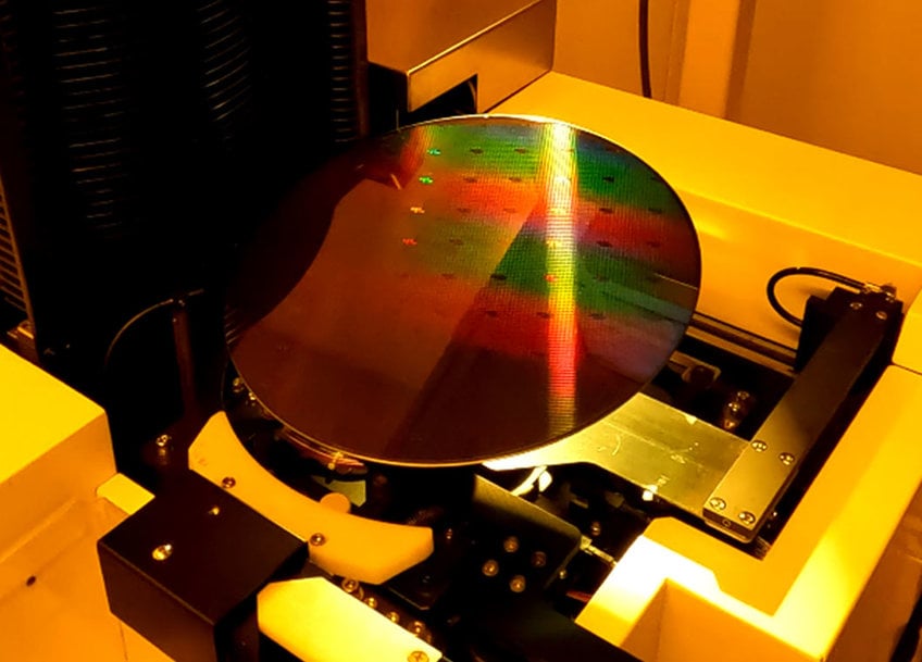
Innoscience Technology, a company founded to create a global energy ecosystem based on high-performance, low-cost gallium-nitride-on-silicon (GaN-on-Si) power solutions, will exhibit for the first time in Europe at the world's largest Power Electronics conference, PCIM Europe - 10 – 12 May 2022, Nuremberg Messe, Nuremberg, Germany.
Dr Denis Marcon, General Manager, Innoscience Europe, has been selected as a speaker at this prestigious international event. The title of his presentation is: Slashing the last barriers for the widespread adoption of GaN-based power transistors
12:30 - 12:50PM, May 10th 2022, Industry Forum, Booth 6-246
He comments: "Many electronic engineers already understood the benefit of using GaN-based transistors in their systems as they can make more efficient, more compact, lighter and even more reliable power electronic systems by using GaN-based transistor with respect to what is possible with traditional Silicon devices. Yet, there are two barriers to overcome for the wide spreading of GaN technology: high price and security of supply (i.e. mass manufacturing).
"In this talk, we will present Innoscience’s 8-inch GaN-on-Si e-mode technology and discuss how we have overcome the aforementioned barriers hindering the large adoption of GaN-based transistors. We will conclude the talk by giving an overview of applications where Innoscience’s GaN devices (InnoGaN™) have been used and the benefit of using InnoGaN™ transistors instead of traditional Silicon devices."
Innoscience will also exhibit at the event on booth 7-249, showcasing its unique, high and low voltage GaN solutions in applications. The company is the world’s largest Integrated Device Manufacturer (IDM) fully focused on GaN technology, with a monthly capacity of 10,000 8-inch wafers per month (WPM). This capacity is set to grow to 70,000 WPM by 2025.
Additionally, visitors to Innoscience's booth will be able to see designs done in partnership with specialized gate-driver companies Heyday and MindCet. Innoscience's GaN HEMT devices can, of course, be used in conjunction with other gate drivers. The company’s devices range from 30V to 650V and are widely used in in applications from USB PD chargers/adapters to data centers, mobile phones and LED drivers.
Dr Marcon added: “We are excited to welcome visitors to PCIM which is Innoscience's first public showcase in Europe. We will demonstrate the huge capacity we already have - the largest in the world - and a wide portfolio of devices which are available now. Innoscience also has the capability to rapidly design and manufacture in high volumes to support customers' requirements wherever they are located globally.”
www.innoscience.com
