electronics-journal.com
22
'24
Written on Modified on
KEYSIGHT INTRODUCES SYSTEM DESIGNER FOR PCIE AND CHIPLET PHY DESIGNER FOR DIGITAL STANDARDS-DRIVEN SIMULATION WORKFLOWS
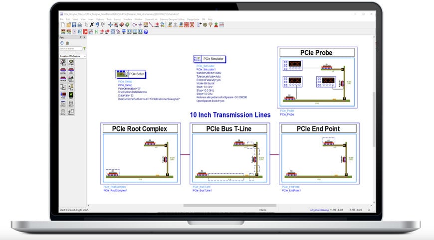
System Designer for PCIe is an intelligent design environment for modelling and simulating the latest PCIe Gen5 and Gen6 systems.
www.keysight.com

Keysight Technologies introduces System Designer for PCIe®, a new product in the Advanced Design System (ADS) product suite that supports simulation workflows based on industry standards for high-speed, high-frequency digital designs. System Designer for PCIe is an intelligent design environment for modelling and simulating the latest Peripheral Component Interconnect Express (PCIe) Gen5 and Gen6 systems. Keysight is also improving its electronic design automation (EDA) platform by adding new features to the existing Chiplet PHY Designer tool to estimate chiplet die-to-die link margin performance and Voltage Transfer Function (VTF) compliance measurement.
PCIe is a versatile and essential interface standard across a wide range of electronics industry segments due to its high-speed data transfer capabilities, scalability, and adaptability. Adoption spans from everyday consumer electronics to specialized applications in high-performance computing and critical infrastructure systems.
Complex PCIe designs support multi-link and multi-lane systems that involve a complex analysis setup between RootComplex and End-Point, sometimes incorporating mid-channel repeaters. Designers spend an inordinate amount of time preparing simulations that are prone to mistakes. Simulations often lack vendor-specific algorithmic modelling interface (AMI) simulation models, which are required early in the design cycle for design space exploration. Designers also need assurance that their prototype design will pass compliance testing before hardware fabrication.
Productivity, Workflow, and Compliance Improvement Features
- The System Designer for PCIe® automates the setup for multi-link, multi-lane, and multi-level (PAM4) PCIe systems using a smart design environment. It simplifies simulation setup and reduces time-to-first-insight.
- The PCIe AMI modeller, which supports NRZ and PAM4 modulations, facilitates quick AMI model generation needed for PCIe system analysis. The AMI Model Builder gives designers a wizard-driven AMI model generation workflow to rapidly create models for both transmitters (Tx) and receivers (Rx).
- Streamlined, simulation-driven virtual compliance testing enables designers to ensure design quality. The integrated, simulation-driven PCIe compliance test workflow reduces design costs by minimizing design iterations and shortening time-to-market.
Chiplet PHY Designer Enhancements
- Chiplet PHY Designer is the EDA industry’s first simulation solution for Universal Chiplet Interconnect Express (UCIe) standards, enabling predictions of die-to-die link margin, VTF for channel compliance analysis, and forwarded clock capability. Chiplet PHY Designer includes new design exploration and report generation features that accelerate signal integrity analysis and compliance verification to improve designer productivity and time-to-market.

