
electronics-journal.com
21
'25
Written on Modified on
Keysight unveils seamless photonic circuit solution
Optimizes photonic circuit performance using advanced simulation, streamlines workflows with holistic automation, and ensures manufacturing readiness through process design kit customization and real-world data integration.
www.keysight.com
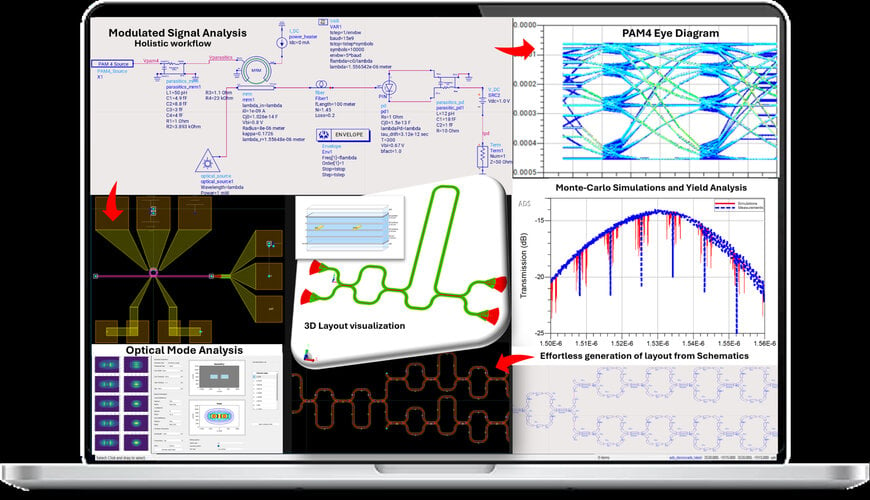
Keysight Technologies, Inc. announces the launch of Photonic Designer, an innovative photonic design automation (PDA) software solution engineered to provide unparalleled accuracy and compliance-driven design validation. Designed for photonics design engineers, this solution enables streamlined workflows from concept to simulation, emulation, and manufacturing, addressing the challenges of fragmented tools, inconsistent simulation precision, and increasing compliance demands.
Photonics design engineers often face challenges with scattered tool chains and simulation discrepancies that hinder efficiency and precision. Traditional workflows require engineers to switch between multiple software platforms, making it challenging to ensure design consistency. Keysight’s Photonic Designer, part of the Advanced Design System (ADS) suite of tools, eliminates these inefficiencies by offering a comprehensive, physics-driven simulation environment that accurately predicts real-world circuit performance. Keysight tools also support an open, interoperable workflow ecosystem for maximum flexibility.
Photonic Designer integrates real-world measurement data directly into the simulation workflow, to optimize models and streamline compliance and validation.
This allows engineers to:
- Verify designs against industry modulation standards before fabrication
- Use Models with best-in-class simulators to ensure accurate, confident, robust designs
- Ensure seamless compatibility with foundry PDKs to avoid costly iterations
- Optimize photonic model variables to match foundry processes to align with manufacturing conditions
- Automate and accelerate design verification, reducing go-to-market time
The software is designed to streamline pure optical and combined electrical-optical-electrical workflows for circuit design, providing an intuitive interface for effortless circuit design and layout generation. Engineers can simulate, validate, and optimize photonic circuits while ensuring compliance with stringent design rules, guaranteeing precision and reliability.
To further enhance the design process, CompoundTek, a leading provider of photonics foundry services, is offering a Photonic Designer PDK for Keysight ADS users, for their silicon photonics process. This collaboration enables engineers to develop PICs with foundry-verified components, ensuring a seamless transition from design to fabrication.
www.keysight.com
