
electronics-journal.com
17
'25
Written on Modified on
Advanced Chiplet Integration Center for European ASIC Development
Avnet ASIC and Bar-Ilan University are establishing a joint R&D hub to develop 2.5D and 3D chiplet integration based on advanced foundry nodes for European semiconductor applications.
www.avnet.com
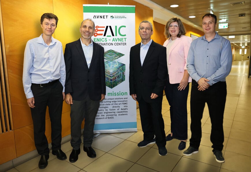
Avnet ASIC, a division of Avnet, has entered a strategic collaboration with Bar-Ilan University to create an Advanced Chiplet Innovation Center focused on next-generation semiconductor integration. Scheduled to open in 2026 at Avnet ASIC’s facility, the center will develop 2.5D and 3D chiplet solutions aligned with advanced TSMC technology nodes, addressing growing demand in the European ASIC market.
Combining industrial ASIC development with academic architecture research
The initiative brings together Avnet ASIC’s experience in ASIC design, physical implementation, and advanced packaging with the research capabilities of Bar-Ilan University’s EnICS Institute, which focuses on advanced semiconductor architectures. The collaboration is structured to translate academic research into deployable chiplet-based designs, rather than operating as a purely exploratory research program.
By co-locating engineers and researchers, the center is intended to function as a practical development environment where architectural concepts can be evaluated against real-world constraints such as manufacturability, reliability, and compliance with advanced process design rules.
Responding to Europe’s demand for advanced chiplet architectures
European semiconductor activity has increased through a mix of public funding initiatives and private investment, particularly among fabless companies targeting automotive, industrial, and high-performance computing applications. These segments increasingly rely on chiplet architectures, 2.5D interposers, and 3D stacking to balance performance, power efficiency, and form-factor limitations that are difficult to achieve with monolithic designs.
The new center is positioned to support these requirements by developing heterogeneous integration approaches compatible with advanced manufacturing standards, while allowing design flexibility for regional customer needs within the European ASIC ecosystem.
Technical focus on 2.5D and 3D heterogeneous integration
Work at the center will concentrate on integrated chiplet packaging using advanced process nodes, with emphasis on electrical and mechanical co-design. Technical activities include simulation-driven optimization, power integrity analysis, thermal modeling, and signal integrity verification, all of which are critical for multi-die systems operating at high bandwidth and power density.
Verification methodologies for chiplet-based architectures will also form a core part of the program, addressing challenges such as die-to-die interfaces, thermal coupling, and system-level reliability. These capabilities are essential for moving chiplet concepts from prototype to production-ready ASIC platforms.
A structured pathway from research to deployment
Beyond technical development, the collaboration establishes a model for closer industry–academic integration. Bar-Ilan University researchers gain direct access to industrial design flows and constraints, while Avnet ASIC can incorporate emerging architectural research into its development processes.
This structure is intended to reduce development risk for European fabless companies by validating advanced integration concepts earlier in the design cycle, shortening the path from research results to manufacturable chiplet-based systems built on globally accepted process technologies.
www.avnet-asic.com
