
electronics-journal.com
15
'26
Written on Modified on
Accelerated Radiation Testing for Microelectronics
Northrop Grumman demonstrates compact radiation-testing technology under DARPA program to shorten qualification cycles for space and nuclear microelectronics.
www.northropgrumman.com
Northrop Grumman has demonstrated a laboratory-scale radiation testing environment that significantly reduces the time required to qualify microelectronics for use in space systems and nuclear facilities, where exposure to high-energy radiation is unavoidable.
Why radiation testing is a bottleneck
Microelectronics deployed in satellites, deep-space missions, and nuclear infrastructure must be resistant to single-event effects (SEE), where high-energy particles can trigger transient faults or permanent damage in semiconductor devices. Qualification against these effects traditionally relies on heavy-ion radiation testing, which in the United States is limited to four national facilities. As a result, access constraints can extend testing schedules from months to several years, delaying system deployment and upgrades.
DARPA ASSERT program context
The demonstration was conducted under the Defense Advanced Research Projects Agency’s DARPA Advanced Sources for Single-event Effects Radiation Testing (ASSERT) program. ASSERT seeks to replace reliance on large accelerator facilities with compact, laboratory-based alternatives capable of reproducing relevant radiation conditions for SEE evaluation.
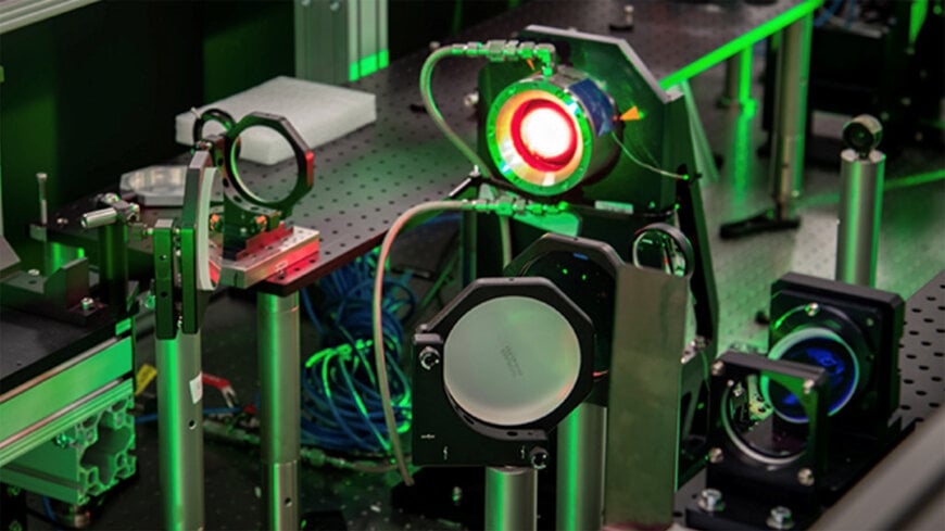
Laser plasma accelerator approach
Northrop Grumman’s approach uses laser plasma accelerator (LPA) technology to generate high-energy electron beams in a significantly smaller footprint than conventional accelerators. The system was developed in collaboration with Lawrence Berkeley National Laboratory and Vanderbilt University, leveraging work at Berkeley Lab’s BELLA Center, which specializes in LPA research.
LPAs accelerate electrons using intense laser pulses interacting with plasma, enabling compact sources that can be installed in secure laboratory environments. According to the company, this setup can reproduce the randomized radiation conditions associated with space and nuclear environments, allowing SEE testing without transporting sensitive components to national facilities.
Measurable impact on test cycles
Northrop Grumman reports that the technology enables up to a tenfold reduction in the combined design, test, and deployment timeline for radiation-hardened microelectronics. By moving testing closer to development teams and removing facility wait times, qualification cycles can be reduced from years to months. The system also supports testing of packaged, stacked, and 3D-heterogeneous devices, which are increasingly common in high-performance and space-grade electronics but difficult to evaluate with existing laser-based surrogate methods.
Applications and technical relevance
The accelerated testing capability is relevant for satellite payloads, deep-space observatories, nuclear monitoring systems, and defense platforms where reliability under radiation exposure is a design requirement. The ability to test advanced device architectures locally also supports faster iteration of microelectronics used in national security and commercial space programs.
Industry context
While conventional heavy-ion facilities remain the benchmark for SEE testing, compact accelerator-based approaches such as LPAs are being evaluated across the sector for their ability to increase test availability and throughput. ASSERT provides a common framework for assessing whether these alternatives can meet established radiation qualification criteria, rather than replacing standards with new ones.
By integrating compact radiation sources into secure laboratories, the demonstrated system addresses a structural constraint in the microelectronics qualification process, with implications for supply chain resilience and deployment timelines in radiation-critical industries.
www.northropgrumman.com
