
electronics-journal.com
19
'26
Written on Modified on
Keysight adds AI modeling toolkit for faster PDK development
The new software module automates parameter extraction for compact device models, supporting DTCO workflows for advanced-node, RF and power semiconductors.
www.keysight.com
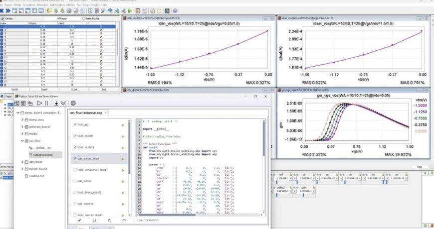
The Machine Learning Toolkit accelerates model development from weeks to hours.
As semiconductor devices shift toward gate-all-around architectures, wide-bandgap materials, and chiplet-based integration, compact model creation and parameter extraction have become major schedule bottlenecks for design enablement. Keysight Technologies has introduced a Machine Learning Toolkit within its Keysight Device Modeling Software Suite to accelerate device modeling and Process Design Kit (PDK) development.
Why modeling and extraction are slowing down advanced nodes
Advanced architectures such as gate-all-around transistors (GAA), heterogeneous integration approaches including chiplets and 3D stacking, and the adoption of GaN and SiC are raising the number of operating conditions and secondary effects that models need to capture. In many flows, developers still rely on compact physical models and manual tuning, where hundreds of coupled parameters must be adjusted across multiple bias, temperature, and signal conditions.
This manual process can take weeks, particularly when the best fit depends on iterative expert judgement rather than a repeatable optimization mechanism. With design schedules tightening, the industry has been pushing toward more automated model parameter extraction workflows that can generate predictive models faster for both device and circuit teams, especially in DTCO programs.
Machine learning-driven extraction within Device Modeling MBP 2026
Keysight’s Machine Learning Toolkit is delivered as part of the latest release of its Device Modeling Software Suite and is implemented within Device Modeling MBP 2026. The toolkit includes an ML optimizer, automated extraction flows, and supporting utilities intended to replace time-intensive manual extraction loops with ML-based optimization using neural network architectures.
Keysight states that the new approach can reduce overall model development and extraction time from weeks to hours, with the goal of enabling faster deployment of PDKs and faster DTCO application development.
From hundreds of manual steps to automated global optimization
A key technical focus of the toolkit is the reduction of the parameter extraction workflow itself. In traditional flows, model engineers may execute more than 200 individual extraction steps, iteratively adjusting parameters as results drift across conditions. Keysight’s automated extraction flow is positioned to cut this to fewer than 10 steps, and in one described configuration to around five to six automated steps.
Within this process, the toolkit supports global optimization of more than 80 parameters in a single pass. The extraction approach is designed to capture secondary effects, temperature variation, and dynamic behavior while reducing the need for repeated manual retuning. The resulting models are positioned for use across DC, RF, and strong-signal applications.
Integration into existing EDA automation pipelines
The toolkit is designed to integrate with Keysight’s Device Modeling Platform and supports Python-based customization. This matters in environments where modeling teams need to standardize and version flows across process nodes and device families, and where model generation must connect cleanly to validation datasets and PDK release pipelines.
In that sense, the module is positioned as an enabler for a more automated “model-to-PDK” pipeline, where extraction recipes can be reused and adapted instead of rebuilt for each new process generation.
Technology coverage: FinFET, GAA, GaN, SiC and bipolar devices
Keysight positions the Machine Learning Toolkit as adaptable across multiple device technologies, including FinFET and GAA transistor nodes, as well as GaN and SiC wide-bandgap devices and bipolar devices. The stated intent is reproducibility across process nodes, with reusable workflows that can be applied to multiple device types rather than tailored each time manually.
For semiconductor teams supporting mixed portfolios across advanced logic, RF front-end, and power devices, this type of workflow portability directly impacts the speed of design enablement and how quickly validated models can be delivered into circuit design environments.
DTCO impact framed in shorter PDK cycles
Keysight links the toolkit directly to DTCO efficiency by shortening the feedback loop between device modeling and circuit design. The release positions this as a path to reduce PDK development cycles from weeks to days by speeding parameter extraction, improving model predictiveness, and automating steps that typically require repeated expert intervention.
In practical use, this supports faster iteration between the component level and the circuit level, particularly in advanced-node design programs where PDK readiness is tightly coupled to tape-out schedules and where model accuracy needs to hold across wider operating envelopes.
www.keysight.com
