
electronics-journal.com
16
'26
Written on Modified on
Mass-Produced HBM4 Boosts AI Datacenter Memory Bandwidth
Samsung Electronics begins industry-first commercial shipments of sixth-generation high-bandwidth memory for AI and HPC workloads.
semiconductor.samsung.com
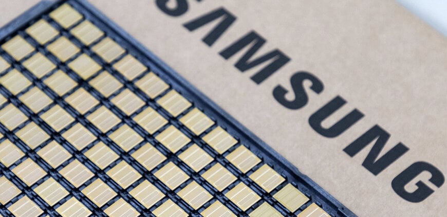
Samsung Electronics has started mass production and commercial shipments of HBM4, a next-generation high-bandwidth memory designed to meet escalating data throughput demands in artificial intelligence (AI) computing and high-performance computing (HPC) systems. The chips deliver a significant performance uplift over previous memory generations, targeting datacenter applications and advanced AI accelerators.
Next-Generation Memory for AI Workloads
HBM4 is the fourth iteration of high-bandwidth memory, intended to address the “memory wall” bottleneck that can limit processor performance by restricting data movement between memory and compute units. The new HBM4 stacks use a sixth-generation 10 nm-class DRAM process paired with a 4 nm logic base die, which Samsung says enables improved yield and performance without redesigns as production scales.
In its initial configurations, HBM4 delivers a consistent transfer speed of 11.7 gigabits per second (Gbps) per pin, exceeding the JEDEC HBM4 baseline of ~8 Gbps and offering about 22 % faster performance than Samsung’s previous HBM3E generation. Peak speeds of up to 13 Gbps are achievable under certain conditions, helping to mitigate data throughput bottlenecks typical in large-scale AI model training and inference.
Bandwidth and Capacity Enhancements
The architecture’s doubled pin count (from 1,024 to 2,048 I/O pins) supports a maximum memory bandwidth of about 3.3 terabytes per second (TB/s) per stack, approximately 2.7 times that of the prior HBM3E generation. Initial capacity offerings include 24 GB and 36 GB stacks built with 12-layer TSV (through-silicon via) technology, with 48 GB configurations planned using 16-layer stacking.
Efficiency and Thermal Management
To offset the power and thermal challenges associated with increased I/O throughput, Samsung has integrated low-voltage TSVs and optimized power distribution networks, resulting in a reported 40 % improvement in power efficiency over HBM3E. The design also targets 10 % better thermal resistance and 30 % improved heat dissipation, factors critical for sustaining performance in dense AI accelerator environments.
Production and Roadmap
Samsung positions HBM4 as a foundational memory technology for AI and datacenter computing, citing co-optimization between its memory and foundry businesses, extensive advanced packaging capabilities, and an integrated supply chain to support demand. The company also plans to expand HBM4 production capacity and expects HBM sales to grow significantly in the coming year. Sampling of the next evolution, HBM4E, is expected in the second half of 2026, with custom HBM solutions slated for delivery in 2027.
Technical Application Context
For engineers and system architects working on AI accelerators, HPC clusters, or data-intensive platforms, HBM4’s increased per-stack bandwidth and enhanced energy efficiency can reduce memory bottlenecks, improve compute utilization, and support larger model footprints without compromising thermal or power constraints. Its adoption in next-generation GPU and ASIC memory subsystems could shift performance ceilings for exascale AI tasks.
www.samsung.com
