
electronics-journal.com
20
'26
Written on Modified on
Keysight Software Targets 3DIC Interconnect Design Bottlenecks
New EDA workflow automates chiplet interconnect modelling and validation to support high-density semiconductor packaging used in AI and data centre hardware.
www.keysight.com
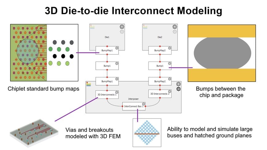
The 3D Interconnect Designer simplifies the design of high-speed 3D interconnects for chip bridges and interposers.
Advanced semiconductor packaging increasingly relies on stacked dies and chiplet architectures, where electrical behaviour depends on complex vertical interconnections. In this context, Keysight Technologies introduced the 3D Interconnect Designer within its Electronic Design Automation portfolio for modelling and validating multi-die and 3DIC structures.
Managing multi-die routing complexity
Chiplet-based processors used in AI infrastructure and data-centre accelerators require detailed modelling of vias, transmission lines, solder balls and microbumps. Traditional manual optimisation forces multiple design iterations because signal integrity and power integrity must be verified across tightly packed geometries.
The 3D Interconnect Designer provides a dedicated workflow for designing and optimising these structures, including complex bases such as hatched or grooved geometries used in interposers and bridge technologies. Early validation reduces repeated redesign cycles that typically extend development timelines in advanced packaging within the semiconductor design supply chain.
Simulation aligned with emerging standards
The software supports compliance checks using interconnect standards, including UCIe and BoW, alongside electrical verification methods such as Voltage Transfer Function (VTF) analysis. Electromagnetic simulation models electrical behaviour across printed circuit boards and package structures, allowing engineers to evaluate performance before fabrication.
By identifying signal and power integrity issues earlier in the design phase, the approach limits late-stage redesigns and improves first-pass design success rates.
Integration with broader design environments
The tool operates both as a standalone application and within the Keysight EDA environment. Combined with Chiplet PHY Designer, it enables coordinated development of chiplet interfaces and 3D interconnect structures in multi-die systems.
Automating interconnect modelling and validation shifts development effort from manual optimisation toward simulation-driven verification, shortening design cycles for high-performance computing and data-centre semiconductor platforms.
www.keysight.com
