
electronics-journal.com
04
'26
Written on Modified on
Keysight Supports GlobalFoundries Silicon Photonics Process Technology
Keysight Technologies has integrated support for GlobalFoundries' silicon photonics process into its Advanced Design System to enable electro-optical-electrical system simulation.
www.keysight.com
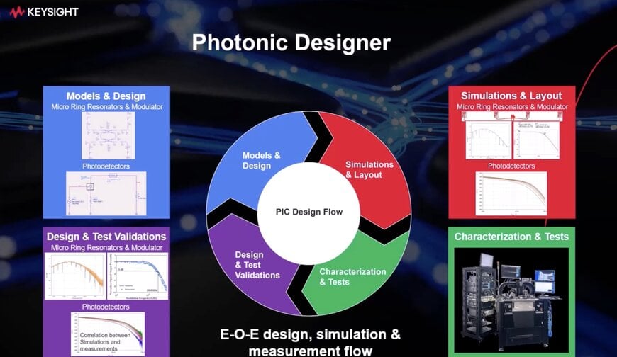
Keysight Technologies has announced support for GlobalFoundries’ (GF) silicon photonics process technology within its Advanced Design System (ADS) Photonic Designer. This integration expands Keysight's foundry ecosystem for photonic integrated circuit (PIC) development. The updated capability allows designers to transition from PIC design to full electro-optical-electrical (EOE) system simulation within a single environment, validating photonic circuit performance at the optical link level prior to tapeout.
Multi-Domain Verification Challenges
As silicon photonics transitions into volume production across data centers, artificial intelligence (AI) infrastructure, and optical communications, engineers face the challenge of confirming PIC performance within an EOE system. Traditional workflows separate these design and simulation phases, requiring engineering teams to move between distinct PIC design tools and system simulation platforms. This operational separation introduces design risk and delays validation until late in the product development cycle.
Process Design Kit Integration and System Insights
The Process Design Kit (PDK) for ADS Photonic Designer connects PIC design with system-level EOE simulation. Engineers can design photonic circuits on the GF platform and validate complete optical link behavior, including eye diagram analysis and signal integrity metrics such as transmission dispersion eye closure quaternary (TDECQ), without transitioning between software tools. The PDK is built on physics-based models aligned to GF’s silicon photonics process, which ensures that PIC simulations correlate to fabricated silicon while verifying channel link performance.
High-Speed Optical Interconnect Development
These PIC and system capabilities apply to high-speed optical interconnect architecture development, as well as subsequent stages where photonic and electronic performance must be verified concurrently. Engineers developing optical transceivers and co-packaged optics can utilize Keysight FlexDCA oscilloscope software during the design phase to establish simulation-to-measurement correlation and obtain predictive results.
Technical and Operational Benefits
The integrated PDK delivers specific functional updates to the design workflow:
- Accelerated Design Initiation: Foundry-aligned, physics-based models for the GF silicon photonics process are available for immediate use, eliminating the need to construct or calibrate component libraries from scratch.
- Pre-Tapeout Compliance: Simulating with Keysight instrument software, FlexDCA-based measurements, and TDECQ analysis reduces design-to-test correlation variables to verify predictive results before manufacturing.
- Early Architecture Evaluation: Moving system-level insight earlier into the development lifecycle allows engineers to evaluate how PIC performance impacts the optical link during initial architecture development, reducing design iterations and time to market.
Edited by Romila DSilva, Induportals Editor, with AI assistance.
