
electronics-journal.com
10
'26
Written on Modified on
Top-Side Cooled Silicon Carbide MOSFETs in QDPAK
Nexperia introduced high-voltage wide-bandgap semiconductors featuring a surface-mount configuration designed to optimize thermal dissipation in power-dense systems.
www.nexperia.com
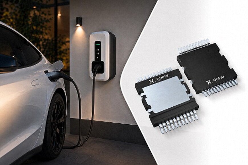
A new portfolio of 1200 V silicon carbide MOSFETs utilizing top-side cooled surface-mount packaging addresses heat dissipation limitations in high-voltage power conversion systems. By establishing a direct die-to-heatsink thermal path from the top side of the package, these devices reduce reliance on the printed circuit board as the primary heat-spreading path, allowing the semiconductor and board thermal domains to be managed independently. This wide-bandgap technology targets applications including electric vehicle onboard chargers, high-voltage DC-DC converters, electric vehicle charging infrastructure, photovoltaic inverters, uninterruptible power supplies, motor drives, and datacenter power systems.
Compared to conventional D2PAK-7 packaging, top-side cooled packages deliver up to 3 kW higher output power at comparable thermal limits, while providing approximately 40 °C of additional thermal headroom at the same power level. When compared to the existing X.PAK platform, the QDPAK design handles approximately 3 kW higher power at comparable case temperatures and offers around 23 °C of additional thermal headroom at similar power levels.
Scalable Resistance Options and Electrical Characteristics
The product line features both industrial-grade and automotive-qualified variants with drain-source on-resistance options of 17, 30, 40, 60, and 80 mΩ. This scalability allows engineers to select components based on specific thermal and mechanical system constraints.
The electrical characteristics include drain-source on-resistance temperature stability to ensure predictable conduction losses during operation at elevated junction temperatures. The low-inductance package design manages controlled switching behavior, while an integrated Kelvin source pin enables faster commutation and improved switching control to mitigate ringing, electromagnetic interference, and switching transients.
Industry Shift Toward Top-Side Cooling
According to Gaetano Pignataro, Head of SiC & IGBT Product Group at Nexperia, the industry faces thermal, mechanical, and efficiency challenges as power conversion systems become smaller, denser, and require higher power. The integration of 1200 V silicon carbide technology with top-side cooling provides a scalable option designed to address these system-level constraints in next-generation high-power applications.
Additional Context
This section details technical specifications and competitive benchmarking not included in the original product announcement.
The transition to top-side cooled surface-mount packages represents a broader industry trend to replace traditional through-hole packages like TO-247 in high-power densities. Standard bottom-side cooled surface-mount devices transfer heat through the printed circuit board, which limits thermal dissipation due to the thermal resistance of the board substrate material. Top-side cooling bypasses the printed circuit board, allowing direct attachment to a liquid-cooled or forced-air heatsink.
In the 1200 V silicon carbide segment, QDPAK competes directly with established top-side cooled packages such as the TOLT (Transistor Outline Leaded Top-side cooling) package developed by Infineon Technologies and similar top-side cooled formats from STMicroelectronics. For example, a 1200 V SiC MOSFET in a TOLT package offers comparable thermal decoupling benefits, enabling higher power integration per unit volume. Benchmark criteria in this space focus on transient thermal impedance (Zthjc), package parasitic inductance, and creepage/clearance distances. While conventional D2PAK-7 packages exhibit higher thermal resistance to the ambient environment because of board material constraints, both QDPAK and TOLT structures achieve a reduction in junction-to-heatsink thermal resistance, maintaining junction temperatures below the standard 175 °C maximum threshold during continuous high-power operation.
Edited by Evgeny Churilov, Induportals Media - Adapted by AI.
www.nexperia.com
