
electronics-journal.com
24
'26
Written on Modified on
Samsung Introduces Fastest UFS 5.0 Storage for Next-Generation Mobile AI
New memory solution delivers higher speeds, improved efficiency, and compact designs for smartphones, wearables, and XR devices.
semiconductor.samsung.com
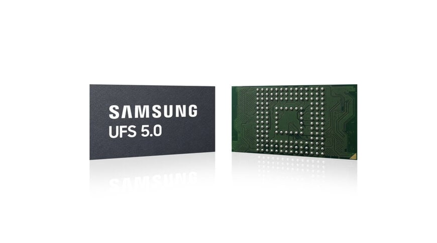
Samsung Electronics announced the development of an embedded universal flash storage architecture to support the mobile data ecosystem and consumer electronics sectors. The technical solution provides high-speed memory processing capabilities for mobile devices and extended reality hardware executing generative artificial intelligence workloads.
Shift to Local Artificial Intelligence Processing
The universal flash storage version 5.0 module functions as an infrastructure component for artificial intelligence computation. Generative artificial intelligence applications increasingly rely on local hardware rather than cloud networks, requiring continuous large-scale data processing within mobile devices. "In the era of on-device AI, storage devices are evolving into a key driver defining AI experiences," said Jangseok Choi, head of Memory Product Planning at Samsung Electronics. "Samsung is setting a new standard for storage on the go and will continue to drive innovation for the next-generation mobile platform market."
Bandwidth and Throughput Specifications
The memory module integrates the embedded interface standard defined by JEDEC. The component achieves a sequential read speed of up to 10.8 gigabytes per second and a sequential write speed of up to 9.5 gigabytes per second. These data transfer rates are more than double the speeds recorded by the previous 4.1 iteration. The increased bandwidth facilitates the rapid storage and execution of large language models directly on the hardware, lowering latency and accelerating response times.
Power Efficiency and Form Factor Metrics
The technical architecture incorporates clock gating and multi-voltage mechanisms to manage power consumption. These integrated technologies improve power efficiency by over 40 percent relative to the predecessor module, reducing the energy required to transfer equivalent data volumes and extending the operational battery lifespan of host devices. Engineers contained the hardware within an ultra-compact package measuring 7.5 millimeters by 13 millimeters by 0.9 millimeters. This physical footprint represents a 16.7 percent reduction in size, optimizing internal space allocation for spatial computing wearables and flagship smartphones. The manufacturer will initiate mass production of the module in capacities up to one terabyte in the fourth quarter.
Additional Context:
This section details technical specifications and competitive benchmarking not included in the original product announcement
The universal flash storage market relies on standardization established by the JEDEC Solid State Technology Association. The 5.0 protocol utilizes the MIPI M-PHY version 6.0 physical layer and the UniPro version 3.0 transport layer to achieve the 10.8 gigabytes per second bandwidth threshold. Within the semiconductor sector, Samsung Electronics competes directly with SK Hynix, Micron Technology, and Kioxia in the deployment of high-speed non-volatile memory. While the previous 4.0 and 4.1 standards saturated at approximately 4.2 to 4.8 gigabytes per second, the transition to the 5.0 architecture enables mobile devices to approach the sequential data transfer rates traditionally associated with peripheral component interconnect express solid-state drives. The standard also implements hardware-level inline hashing and link equalization to preserve data integrity during high-speed transfers.
Edited by Natania Lyngdoh, Induportals editor, assisted by AI.
www.semiconductor.samsung.com
