
electronics-journal.com
20
'26
Written on Modified on
Semiconductor Manufacturing Ceramics for Process Chambers
CeramTec introduces advanced technical ceramics for wafer handling, plasma etching, and thermal management at SEMICON Europa to prevent contamination and thermal degradation.
www.ceramtec-group.com
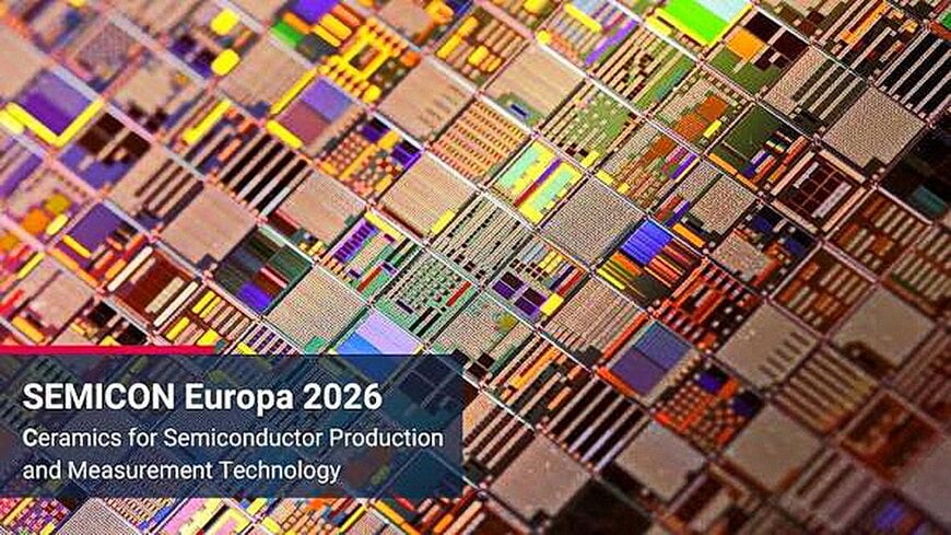
SEMICON Europa, taking place from 10 to 13 November 2026 in Munich, Germany, connects the European semiconductor design and manufacturing supply chain. During the event, technical ceramic components engineered for deposition, plasma etching, wafer transport, and high-vacuum metrology will be presented to address yield loss caused by chemical corrosion and thermal stress.
Core Technology and System Architecture
The presented components utilize silicon carbide, silicon nitride, aluminium nitride, and aluminium oxide formulations tailored for sub-micron process stability. Silicon carbide wafer chucks, end-effectors, and robotic handling arms feature surface roughness values below Ra 0.35 micrometers, preventing mechanical micro-scratching and particle generation during substrate transfer. For chemical vapour deposition, physical vapour deposition, and plasma etching tools, process chamber linings, gas distribution plates, and focus rings rely on dense aluminium oxide and silicon carbide to withstand continuous fluorine- and chlorine-based plasma erosion. Precision gas nozzles and injectors maintain mechanical flatness tolerances below 2 micrometers to ensure uniform laminar gas dispersion across wafer surfaces. For complex, mass-optimized geometries, additively manufactured ROCAR 3D ceramic structures provide high dimensional stiffness without adding structural mass to moving stages.
Industry Applications
These ceramic solutions serve front-end semiconductor fabrication plants, advanced packaging facilities, and metrology equipment manufacturers. Specific operational applications include electrostatic chuck clamping, high-temperature chemical vapour deposition chambers, radio-frequency electrode isolation, and high-vacuum metrology stages. Deploying chemically inert ceramic assemblies eliminates metallic ion contamination within critical process zones, ensuring batch-to-batch repeatability and extending maintenance intervals on automated wafer lines.
Operational Impact and Performance Metrics
Thermal management components mitigate spatial temperature gradients that introduce thermal stress and dopant diffusion variances. Aluminium nitride ceramic heating plates achieve a uniform surface temperature distribution within plus or minus 0.5 degrees Celsius, while aluminium nitride heat sinks and ceramic substrates dissipate heat fluxes away from power electronics in tool control units. Hermetically sealed ceramic feedthroughs preserve electrical isolation under high-voltage conditions within vacuum chambers operating down to ultra-high vacuum thresholds. These material characteristics prevent mechanical drift, structural bowing, and outgassing under elevated thermal loads.
"In semiconductor manufacturing, precision, purity and process stability are not optional – they are essential," states Dieter Soukup, Sales Director Semiconductors at CeramTec. "Our ceramic materials help manufacturers safely master extreme thermal loads, aggressive chemicals and plasma environments."
Deployment and Integration
The ceramic assemblies integrate directly into standard OEM tool architectures, replacing metallic and quartz fixtures that degrade under fluorine chemistries. Tool integration occurs at Stand 335 in Hall C2 during SEMICON Europa 2026 in Munich, where engineers can assess material specifications and custom dimensional integration parameters for high-temperature and high-vacuum applications.
Edited by Evgeny Churilov, Induportals Media - Adapted by AI.
www.ceramtec-group.com
