
Samsung Adopts Ansys’ Simulation Portfolio to Create Semiconductor Designs to Optimize High-Speed Connectivity
Samsung will employ Ansys’ electromagnetic simulation tool suite to develop state-of-the-art designs, including 5G/6G, on the most advanced process technologies.
Samsung Adopts Ansys’ Simulation Portfolio to Create Semiconductor Designs to Optimize High-Speed Connectivity
- Ansys’ simulation solutions will provide Samsung developers with a comprehensive electromagnetics-aware design flow to improve productivity and reduce design risk
- Samsung designers will benefit from Ansys’ advanced capacity, speed, and integration capabilities to accelerate electromagnetic design cycle times by a factor of 10 and reduce time to market
- Ansys’ cutting-edge design features, such as automatic annotation, will optimize Samsung’s on-chip design through faster, more predictively accurate calculations and modeling
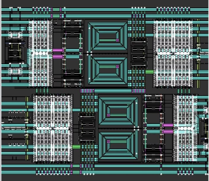
Samsung Foundry will engage Ansys’ industry-leading electromagnetic (EM) simulation tools to develop ultramodern designs, including 5G/6G, on the most advanced chips, nodes, and process technologies. Ansys’ simulation solutions will deliver a comprehensive EM-aware design flow with greater capacity, speed, and integration capabilities for Samsung’s most advanced semiconductor technology, accelerating on-chip design cycle times to boost high-speed connectivity while helping to reduce design error and risk.
Samsung designers will leverage Ansys’ EM design tools, Ansys RaptorX, Ansys VeloceRF, and Ansys Exalto, to help reduce time to market by two to three weeks on smaller designs and up to two months for complex designs. With automation capabilities that optimize calculations and modeling, coupled with larger capacity, Ansys’ software will allow the Samsung team to design at faster speeds with higher fidelity.
“Electronic systems and process technologies are constantly evolving and therefore require leading-edge EM design capabilities,” said Sangyun Kim, corporate vice president of the Foundry Design Technology Team at Samsung Electronics. “We believe that Ansys’ simulation solutions meet these challenges and will deliver the highest level of proficiency for our design needs, while reducing design time, cost, and risk.”
By integrating Ansys’ EM solutions, Samsung designers can model complex on-chip scenarios, including dummy tiles, which comprise millions of metal pieces in a fraction of the time. Additionally, Ansys’ near real-time modelling capabilities safeguard designs from EM interference, which helps significantly lower the risk of chip failure.
“EM is a primary challenge for chip designers as connectivity demands increase and technologies advance worldwide,” said John Lee, vice president and general manager of the electronics, semiconductor, and optics business unit at Ansys. “At Ansys, we ensure that our simulation solutions not only meet these rising demands but remain ahead of them. We are confident that Ansys’ EM design portfolio is well-equipped to serve the Samsung team with the tools they need to optimize their on-chip designs.”
Ansys and Samsung have a long history of collaboration that delivers advanced solutions, including power integrity and electromigration signoff solutions for low-power mobile and high-performance computing applications.
www.ansys.com
