
electronics-journal.com
26
'25
Written on Modified on
Semiconductor Carbon Emission Reduction Using Alternative Process Gases
Samsung Semiconductor outlines its strategy to lower greenhouse gas emissions in semiconductor manufacturing through collaboration on alternative gases and process improvements.
semiconductor.samsung.com
Samsung Semiconductor has introduced a coordinated effort with suppliers and industry partners to reduce carbon emissions from semiconductor manufacturing by adopting alternative etching process gases with lower global warming potential (GWP). This initiative targets high-impact greenhouse gases used in key fabrication steps, aiming to support broader climate goals within the semiconductor industry.
Background and Industrial Context
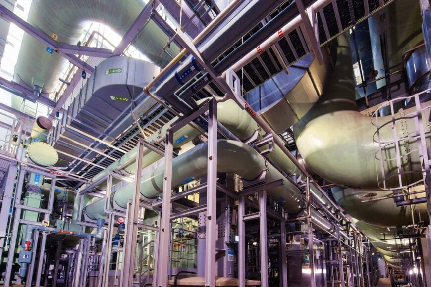
Semiconductor fabrication relies on a range of specialised process gases, particularly in plasma etching operations. Many of these gases, such as perfluorocarbons (PFCs) including CF₄, CHF₃ and C₄F₈, have high GWPs, meaning they contribute disproportionately to Scope 1 greenhouse gas emissions when released or abated inefficiently. Process gases are responsible for approximately 70% of Samsung Semiconductor’s direct (Scope 1) emissions footprint.
In response, Samsung Semiconductor has aligned its practices with net-zero objectives articulated in its 2022 environmental strategy, which sets targets for eliminating both Scope 1 and Scope 2 emissions by mid-century.
Development and Deployment of Alternative Gases
At the SEMICON Japan 2025 trade event (December 17–19, Tokyo), Samsung Semiconductor and Daikin presented a new alternative etching gas known as G2, developed jointly to replace CHF₃ in production processes. The company’s structured development pathway evaluated numerous candidates with supplier partners through material compatibility studies, equipment assessments, in-house lab testing and validation on production lines. This engineering process ensured that alternative gases could meet manufacturing performance criteria while delivering lower environmental impact.
Samsung’s alternative gas portfolio includes:
- G1: Replaces C₄F₈; in use since 2018.
- G3: Replaces CF₄ with near-complete reduction in GWP relative to the conventional gas; deployed across manufacturing sites in 2025.
- G2: Designed to replace CHF₃ with roughly 90% lower GWP; scheduled for application beginning in 2026.
These gases are applicable in the etching steps of semiconductor process flows, where plasma chemistry plays a critical role in pattern transfer and feature definition.
Process Gas Treatment and Scope 2 Reductions
Alongside alternative gases, Samsung Semiconductor operates large-scale process gas treatment systems, notably its Regenerative Catalytic System (RCS), which abates high-GWP emissions from existing gases. RCS units, enhanced with third-generation catalysts, have achieved treatment efficiencies of up to 97% for targeted PFCs. As of 2024, Samsung deployed 52 RCS units, with plans to expand coverage across both existing and new production lines.
The company also collaborates with equipment suppliers to upgrade existing tools for energy efficiency and to inform specification development for new facilities, contributing to reductions in indirect (Scope 2) emissions.
Broader Industry Implications
Samsung’s approach reflects a broader industry trend toward a digital supply chain and manufacturing ecosystem that accounts for environmental externalities of semiconductor processes. By making developed alternative gases available to other fabricators and partners, Samsung positions these materials as shared infrastructure to reduce carbon emissions across supply chains.
The transition to lower-GWP gases, combined with process gas treatment and energy efficiency improvements, represents a measurable step toward decarbonising semiconductor manufacturing — an area that has historically posed challenges due to the unique physical and chemical demands of advanced node fabrication.
Technical Use Cases and Benefits
In practical terms, replacing high-GWP etching gases with alternatives reduces the carbon dioxide-equivalent emissions for each wafer processed. For example, substituting CF₄ with the G3 gas nearly eliminates the GWP contribution from that chemical source. The G2 gas’s ~90% GWP reduction relative to CHF₃ further diminishes the direct climate impact of etch operations. These changes can also help manufacturers align with regulatory and stakeholder expectations for greenhouse gas reporting under protocols such as the GHG Protocol.
Samsung Semiconductor continues to invest in research into low-GWP chemistry, advanced treatment systems and cross-industry collaboration to improve environmental performance. These efforts aim to support net-zero operational targets and to catalyse broader adoption of climate-focused manufacturing practices within the semiconductor industry.
www.semiconductor.samsung.com
