
electronics-journal.com
30
'26
Written on Modified on
AMD's systems-on-chip integrate memory directly
New AMD's SoC integrates up to 32GB of LPDDR5X memory, delivering higher bandwidth, reduced board area and accelerated system development.
www.amd.com
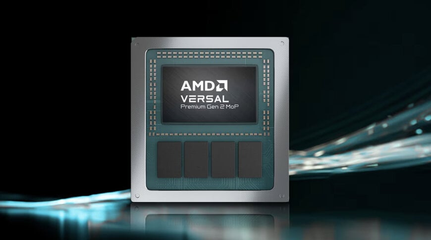
AMD announced the release of its adaptive system-on-chip devices featuring memory integrated directly into the packaging architecture. This technical approach supports data-intensive workloads across physical artificial intelligence, telecommunications networking, and aerospace applications by combining logic and memory within a single component.
Memory Integration and Spatial Efficiency Requirements
The integration of up to 32 gigabytes of LPDDR5X memory directly into the adaptive system-on-chip package changes how engineers design high-bandwidth systems. By moving memory on-package, the architecture delivers up to 288 gigabytes per second of bandwidth while reducing required circuit board area by up to 60 percent compared to discrete memory implementations. This spatial efficiency allows system architects to utilize form factors that are difficult to achieve with external memory routing, such as Enterprise and Datacenter Standard Form Factor configurations and 3U VPX systems used in secure communications and defense acceleration. Pre-validated on-package memory interfaces also eliminate the need for high-speed memory routing across the printed circuit board, reducing simulation and validation requirements.
High-Speed Connectivity and Security Hardware
The hardware ecosystem requires rapid data movement and robust security protocols for industrial deployments. The devices integrate Compute Express Link 3.1 and Peripheral Component Interconnect Express 6.0 at 64 gigabits per second using hardened intellectual property blocks. This connectivity allows the systems to scale memory resources up to 9,000 megabits per second and interface with external memory pooling modules when paired with central processing units. For security, the architecture implements Integrity and Data Encryption at the link layer, alongside DDR memory encryption in the integrated controllers to secure data at rest without consuming programmable logic gates. Hardened 400-gigabit high-speed cryptographic engines process secure communications while maintaining data throughput.
Thermal Resilience and Component Longevity
Sumit Shah, head of product management and marketing for the Adaptive and Embedded Computing Group at AMD, stated that integrating memory on the package allows customers to design systems based on operational requirements rather than external memory constraints. The devices operate within an industrial temperature range of negative 40 degrees Celsius to 110 degrees Celsius, supporting continuous infrastructure deployments. The implementation of LPDDR5X memory includes 15-plus-year lifecycle support, which isolates product availability from the shorter refresh cycles typical of high-bandwidth memory used in data center applications. Standard devices from the series are actively shipping to support development, while the integrated memory components are scheduled for sampling in late 2026, with production shipments following in the subsequent year.
Additional Context:
This section details technical specifications and competitive benchmarking not included in the original product announcement
The approach of integrating memory directly onto a programmable logic or adaptive system-on-chip package is a defined strategy in the semiconductor architecture industry to bypass external memory bottlenecks. Intel addresses this hardware ecosystem requirement with its Agilex M-Series field-programmable gate arrays, which incorporate in-package HBM2e memory to achieve bandwidths exceeding 800 gigabytes per second. While the Intel approach utilizes high-bandwidth memory optimized for maximum throughput in data centers, the AMD implementation utilizes LPDDR5X to balance bandwidth with extended component lifecycles and lower thermal constraints suitable for ruggedized edge and industrial environments. Benchmark comparisons between these architectures typically evaluate total memory bandwidth, the power consumption per bit transferred, and the spatial volume required for the final integrated package assembly.
Edited by Natania Lyngdoh, Induportals editor, assisted by AI.
www.amd.com
