
electronics-journal.com
11
'26
Written on Modified on
Compact Photorelays for Semiconductor Automated Test Equipment
Toshiba introduces high-current solid-state relays in a miniature package to improve switching accuracy and circuit board density in hardware testing environments.
www.global.toshiba
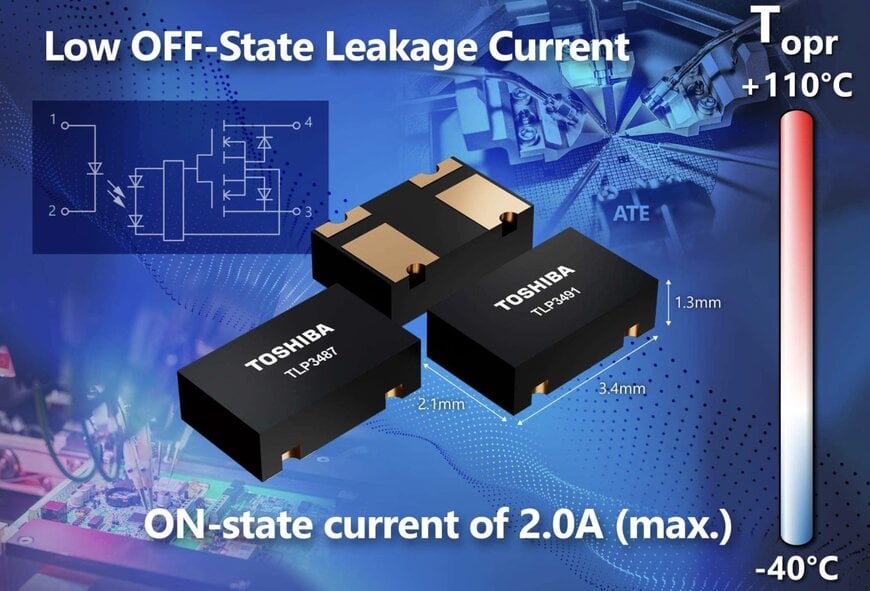
Toshiba Electronics Europe introduces the TLP3487 and TLP3491 photorelays, engineered to deliver precise switching and reliable signal isolation within semiconductor test systems. These components are specifically utilized in automated test equipment (ATE), measuring instruments, and high-speed logic, memory, and SoC testers to manage critical power and signal routing.
Operational Challenges in Device Testing
Semiconductor test systems operate by applying specified voltages and currents to individual pins of a device under test to verify functional integrity. This process requires precise and reliable switching of the power and signal paths connected to each pin. Solid-state relays utilizing MOSFET outputs are standard components for this task. However, a primary technical challenge is off-state leakage current, which can distort measurement results. Concurrently, routing power supplies and controlling loads requires components capable of sustaining high electrical currents, forcing engineers to balance current capacity with measurement isolation.
Technical Performance and Device Architecture
The TLP3491 and TLP3487 components address these operational requirements by combining a high maximum on-state current of 2.0 A with minimal off-state leakage. Through an optimized MOSFET output stage design, the TLP3487 limits leakage to 1 nA at 40 V, while the TLP3491 restricts leakage to 10 nA at 60 V. This mechanism ensures that diagnostic signals remain clean and isolated during testing phases. The specified operating temperature range for these devices spans -40 °C to +110 °C, ensuring stability under heavy thermal loads common in dense testing configurations.
Hardware Integration and Space Efficiency
In high-current applications, engineers historically combine multiple switching devices, which inherently increases both the required circuit board area and the cumulative off-state leakage current. By utilizing a single relay capable of handling 2.0 A, system designers can eliminate redundant components. The devices are packaged in a P-SON4 format measuring 3.4 mm by 2.1 mm by 1.3 mm. This geometry yields a footprint that is approximately 74 percent smaller than standard 2.54SOP4 photorelays and 84 percent smaller than 2.54SOP6 devices, directly supporting the high-density routing requirements of modern automated test equipment.
Additional Context
This section details technical specifications and competitive benchmarking not included in the original news release.
Within the automated test equipment sector, solid-state switching is highly competitive, with established alternatives such as the Panasonic PhotoMOS series and Omron G3VM relay families. Benchmarking these components typically involves measuring the trade-off between load current capacity, off-state leakage, and physical package size. While competitive products offer extremely low leakage currents in sub-miniature SON or VSON packages, achieving a continuous 2.0 A load rating historically requires adopting larger SOP4 or SOP6 packages. By maintaining the 2.0 A specification within the 3.4 mm by 2.1 mm P-SON4 footprint, these components provide a measurable density advantage for hardware engineers designing multi-channel, high-pin-count semiconductor test arrays.
Edited by Aishwarya Mambet, Induportals Editor, with AI assistance.
www.toshiba.com
