
electronics-journal.com
02
'26
Written on Modified on
TRUMPF Showcases Integrated AI Chip Cooling Technology at Semicon Taiwan 2026
Ultrashort-pulse lasers create microscopic cooling structures directly within chip stacks, addressing heat dissipation challenges in advanced semiconductor packaging.
www.trumpf.com
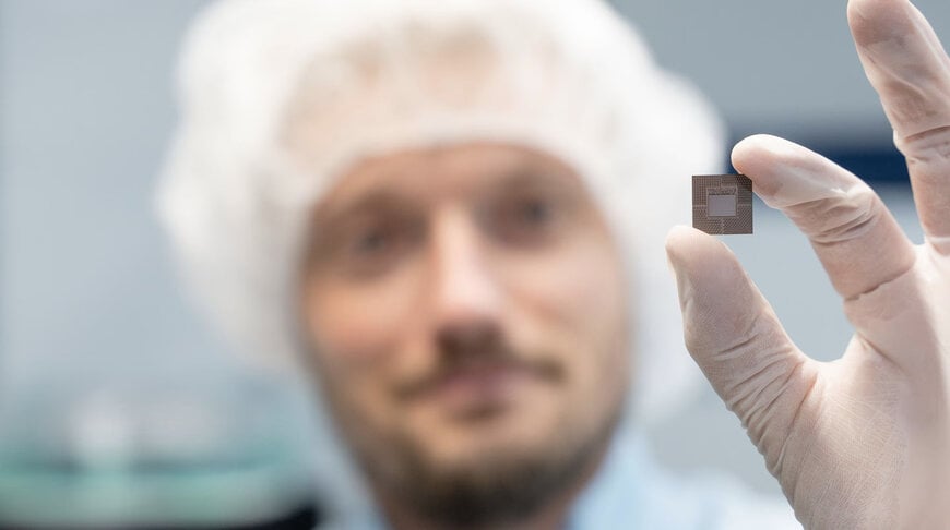
TRUMPF is advancing the semiconductor thermal management ecosystem by introducing a new ultrashort-pulse laser application designed for the direct fabrication of integrated cooling systems within AI processors. This laser ablation technology enables semiconductor manufacturers to produce microscale cooling structures in hard substrate materials, facilitating localized heat dissipation directly within highly dense advanced chip packages.
Addressing Thermal Bottlenecks in Advanced Packaging Architectures
Manufacturers are continually utilizing advanced packaging techniques, combining stacked or densely interconnected chips to increase computing power within minimal footprints. Consequently, heat generation occurs deep inside the chip stack, severely limiting the efficacy of conventional macro-level data center or server rack cooling methods. To maintain processor performance and reliability, semiconductor manufacturers are incorporating microfluidic cooling mechanisms and integrated heat spreaders directly into the device architecture. This strategy necessitates the creation of ultra-fine channels within package substrates, such as silicon carbide and diamond, to dissipate thermal loads exactly where they originate.
Ultrashort-Pulse Laser Processing for Silicon Carbide Substrates
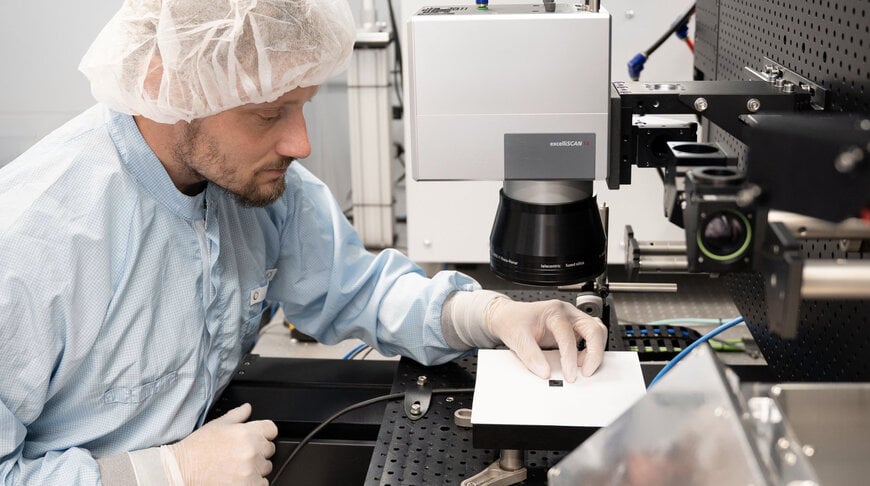
Integrating cooling structures into materials like silicon carbide poses significant manufacturing obstacles. While silicon carbide possesses excellent thermal conductivity suitable for high-demand semiconductor applications, its extreme hardness makes micro-scale fabrication via standard etching processes difficult. TRUMPF addresses this challenge by deploying ultrashort-pulse lasers to ablate the silicon carbide with micrometer precision. High accuracy is critical for maintaining reliable fluid dynamics and thermal transfer within the final cooling component without causing mechanical degradation to the surrounding material.
Industrial Scale Integration and Manufacturing Throughput
At the Semicon Taiwan trade show, TRUMPF demonstrated that this laser application provides the throughput and geometric precision required for volume manufacturing. Cathrin Conrad, Business Development Manager at TRUMPF, notes that heat dissipation acts as a hard limit for high-performance processors, making integrated cooling an absolute necessity. She states, "The combination of high laser power, beam-shaping technology, and our many years of application expertise makes the industrial production of integrated cooling systems in chip stacks possible." In direct comparison to traditional semiconductor etching, the ultrashort-pulse laser methodology achieves at least five times the processing speed while maintaining excellent surface quality and precise micro-channel geometries. This continuous throughput rate enables the semiconductor industry to simultaneously meet quality thresholds and cost-effectiveness requirements for next-generation computing hardware.
Additional Context:
This section details technical specifications and competitive benchmarking not included in the original product announcement
Within the semiconductor manufacturing sector, the fabrication of microfluidic channels in hard, wide-bandgap materials like silicon carbide and diamond has traditionally relied on deep reactive ion etching. While chemical etching is standard for conventional silicon, it struggles with the chemical inertness and material hardness of silicon carbide, resulting in low etch rates and accelerated wear on masking layers. Laser micromachining competitors provide alternative laser systems for wafer dicing; however, the TRUMPF application targets internal device cooling by utilizing specific beam-shaping optics that maximize volumetric ablation rates. By operating in the ultrashort-pulse regime, the system induces cold ablation, which vaporizes the substrate material without transferring residual thermal energy that could induce micro-cracking or warp the semiconductor package. This precise energy delivery mechanism directly accounts for the documented fivefold increase in processing speed over chemical etching while satisfying the strict structural tolerances required for on-chip microfluidic thermal management.
Edited by Natania Lyngdoh, Induportals editor, assisted by AI.
www.trumpf.com
