
electronics-journal.com
15
'26
Written on Modified on
Planar Air Bearing Platforms for Semiconductor Step-and-Scan Applications
ETEL introduces a full air bearing planar platform designed to support next-generation maskless lithography and optical inspection within the semiconductor ecosystem.
www.etel.ch
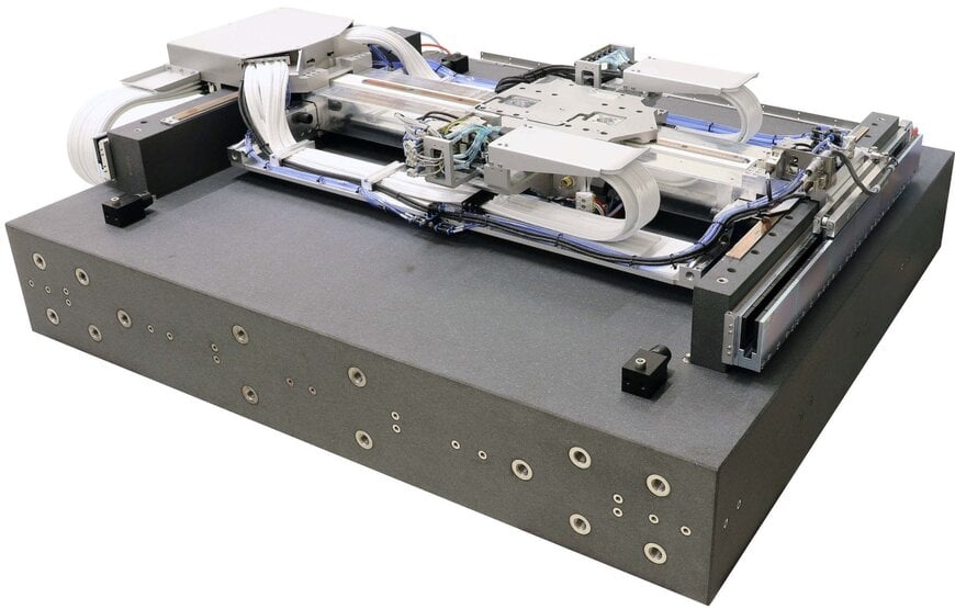
ETEL is releasing the METIS HP, a high-precision XY air bearing stage engineered for step-and-scan semiconductor applications. This motion control platform provides dynamic straightness and speed stability for direct laser writing and high-resolution optical inspection systems handling large-area substrates.
Multi-Degree-of-Freedom Position Measurement
To eliminate thermal drift and ensure spatial accuracy across panel sizes up to 600 mm by 600 mm, the system integrates a multi-degree-of-freedom (mDoF) HEIDENHAIN encoder. This architecture enables projected tool-point measurement, allowing system controllers to emulate a transistor-transistor logic (TTL) position signal as a trigger event. This mechanism serves as an alternative to classical interferometers used for advanced trigger generation, removing the need for carriage-mounted mirrors and mitigating environmental air lensing effects or air perturbations.
Dynamic Metrology and Lithography Specifications
For demanding step-and-scan operations within the semiconductor manufacturing ecosystem, the platform achieves an accuracy of ±150 nm over the complete XY stroke following spatial mapping. It maintains a dynamic straightness of ±150 nm at scanning speeds up to 1 m/s, with maximum acceleration capabilities reaching 20 m/s². These mechanical specifications minimize turnaround times, directly increasing machine throughput for continuous optical processes. Product Manager Stéphane Pellegrini noted that the system's trajectory quality specifically addresses the requirements of advanced optical processing on large-area substrates where consistent scanning velocity is critical.
Focal-Distance Control for Advanced Packaging
High-end inspection routines require rapid and precise focal-distance adjustments to maintain optical clarity. The METIS HP incorporates a high-bandwidth, 4-DoF module that provides fine mechanical control over the Z, tip, tilt, and theta axes, optimizing the platform for advanced packaging inspection tasks. The technology was exhibited at the HEIDENHAIN booth during SEMICON West, which took place October 13–15, 2026, in San Francisco.
Additional Context
This section details technical specifications and competitive benchmarking not included in the original news release.
The market for high-precision XY air bearing stages in semiconductor metrology includes established platforms from manufacturers such as Aerotech (e.g., the PlanarDL series) and Physik Instrumente (PI). Traditional high-end planar air bearing stages frequently rely on laser interferometry to achieve sub-micron accuracy, which can introduce complexities related to atmospheric fluctuations (air lensing) and require rigid, space-consuming mirror configurations.
By utilizing a multi-degree-of-freedom linear encoder capable of TTL signal emulation, the METIS HP provides an alternative measurement topology that reduces these atmospheric dependencies. While competing commercial planar stages routinely achieve scanning speeds of 1 m/s to 1.5 m/s with accelerations exceeding 10 m/s², the METIS HP's ability to maintain a ±150 nm dynamic straightness at 1 m/s, combined with a 20 m/s² peak acceleration, places it at the higher end of the dynamic performance spectrum for non-interferometer-based mechanical positioning systems handling large 600 mm substrates.
Edited by Aishwarya Mambet, Induportals Editor, with AI assistance.
www.etel.com
