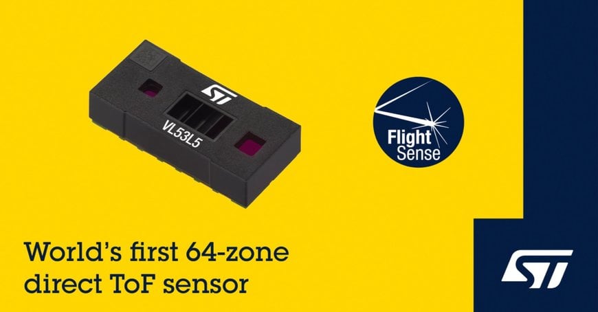
STMicroelectronics Introduces World’s First All-in-One, Multi-Zone, Direct Time-of-Flight Module
STMicroelectronics (NYSE: STM), a global semiconductor leader serving customers across the spectrum of electronics applications, has extended its portfolio of FlightSense Time-of-Flight (ToF) sensors with the world’s first 64-zone device that breaks a scene into separate areas to help an imaging system build the most detailed spatial understanding of a scene.

- Increased camera Field-of-View coverage and spatial resolution enable new features in consumer-electronics imaging systems: touch-to-focus, multiple-target identification, flash dimming, video tracking assistance
- Module integrates Single Photon Avalanche Diode array, wide Field-of-View optics, and low-power on-board processing
This first-of-its-kind product comprises a 940nm Vertical Cavity Surface Emission Laser (VCSEL) light source, a System-on-Chip sensor integrating a VCSEL driver, the receiving array of Single Photon Avalanche Diodes(SPADs), and a low-power 32-bit MCU core and accelerator running sophisticated firmware. TheVL53L5 retains the Class 1 certification of all ST’sFlightSensesensors and is fully eye-safe for consumer products.
Housed in a miniature module, the VL53L5 ToFsensor contains optical elements in the receive aperture that creates 64 ranging zones, unlocking a host of new features and use cases.
“The multi-zone VL53L5 FlightSense direct Time-of-Flight sensor uses our most advanced 40nm SPAD production process to offer outstanding 4m ranging performance and up to 64 ranging zones that help an imaging system build a detailed spatial understanding of the scene,” said Eric Aussedat, General Manager of ST’s Imaging Division. “Delivering 64x more ranging zones than previously available, the VL53L5 offers radical performance improvement in laser autofocus, touch-to-focus, presence detection, and gesture interfaces while helping developers create even more innovative imaging applications.”
With a vertically integrated manufacturing model for its FlightSense sensors, ST builds its SPAD wafers on a 40nm proprietary silicon process in the Company’s state-of-the-art 12” wafer plant at Crolles, France before assembling all of the module components in ST’s back-end plants in Asia. This approach delivers exceptional quality and reliability to customers.
Customer development with the VL53L5 can build on ST’s strong relationships with key smartphone and PC platform suppliers as ST has pre-integrated the sensor onto these platforms. Android and Windows device drivers are also widely available for the FlightSense products. The VL53L5 is in mass production with millions of units already shipped to leading wireless and computer manufacturers.
www.st.com

