electronics-journal.com
17
'21
Written on Modified on
OptiMOS 6 100 V significantly improves technology to set a new industry standard for high switching frequency applications
For modern switch-mode power supplies (SMPS) and battery-powered applications there is a clear trend towards higher efficiency and improved reliability. Supporting this trend, Infineon Technologies AG (FSE: IFX / OTCQX: IFNNY) introduces the OptiMOS 6 100 V with a new power MOSFET technology.

The new technology is specifically optimized for high switching frequency applications such as telecom and solar, where losses are associated with charges (switching) and on-state resistance (conduction). At the same time, due to the best-in-class R DS(on) and wider safe operating area (SOA), it is also ideal for battery-powered applications (BPA) and battery management systems (BMS).
Taking advantage of a novel design concept, the OptiMOS 6 100 V family of MOSFETs comes with improved R DS(on) and industry’s best figures-of-merit (FOMs). It combines the benefits of exceptionally low on-state resistance and superior switching performances. The unique features of OptiMOS 6 allow for easier thermal design and less paralleling, leading to excellent efficiency, improved power density, system cost reduction, and prolonged lifetime.
Especially in the telecom market, OptiMOS 6 is a “game-changer” by achieving 18 percent lower R DS(on) and more than 30 percent improvement in FOMs (R DS(on) x Q g and Q gd), compared to the state-of-the-art OptiMOS 5 . In a 600 W, -(36-60) V to 12 V ZVS buck-boost converter, the OptiMOS 6 in SuperSO8 package with 2.2 mΩ can achieve one percent higher efficiency than OptiMOS 5 BSC027N10NS5 (2.7 mΩ) across the whole load range. This results in a 7 W lower power loss due to improved charges and R DS(on), enabling up to 15 percent higher power density. Among the key benefits, the new technology in the 100 V range allows for lower conduction and switching losses and minimizes the necessity for paralleling parts.
OptiMOS 6 100 V is an energy efficient solution that contributes to a greener world. In the framework of telecom power system, by switching to the new MOSFET technology, the annual electricity saving potential equals the electricity consumption of 170 households. The devices help to reduce the energy consumption by one million Euros over a time span of ten years* .
Availability
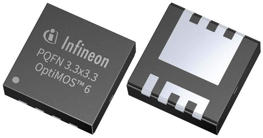
OptiMOS 6 100 V is now available in SuperSO8 5x6 and PQFN 3.3x3.3 packages in a broad range of R DS(on) classes from industry best-in-class to price/performance optimized. More information is available at www.infineon.com/optimos-6-100V.
More information about Infineon’s contribution to energy efficiency: www.infineon.com/green-energy.
*Value given considering average yearly household energy consumption in EU. Statement based on the efficiency gained replacing OptiMOS™ 5 with OptiMOS™ 6 in the primary-side of a 600 W 36…75V to 12V telecom intermediate bus converter at nominal line voltage. Calculated according to typ. average DC power consumption of BBU equipment in telecom power system, in EU country of ~80M people, assuming electricity prices for corporate and their trends, as published by Eurostat.
www.infineon.com

